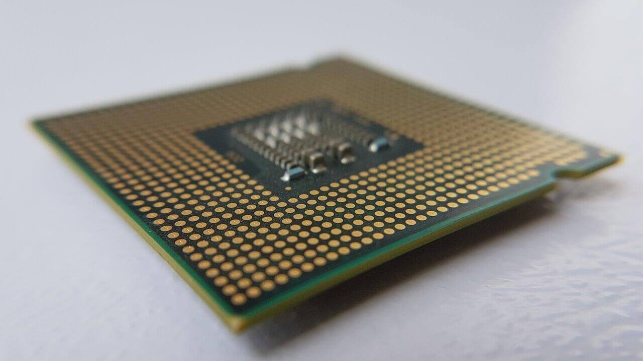
A Quantum Leap in Manufacturing: Our Strategic Partner Achieves Breakthroughs in MLO(multi-layer-organics) Capabilities
In a groundbreaking stride toward innovation, our strategic partner has unveiled a series of remarkable breakthroughs in their manufacturing capabilities for MLO substrates in 2023 with an array of key attributes that redefine the benchmarks for MLO substrate technology.
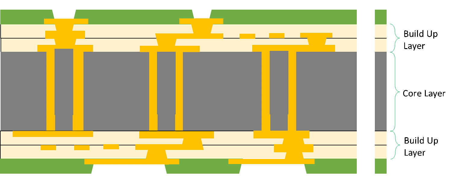
Pushing the Limits: Build-Up Layers Reach New Heights
An impressive build-up layers count of maximum of 11 layers has been achieved, with ongoing development aiming for an 14 layers. With minimum annular ring 10μm. This leap in layering not only expands the design possibilities for semiconductor devices but also enhances the substrate's functionality and performance.
Precision Redefined: Warpage and Flatness Achieve Unprecedented Levels
One of the defining features of this manufacturing breakthrough is the strict adherence to precision standards. The MLO substrates boast a warpage of less than 0.3%, ensuring a level of structural integrity that is crucial for testing applications. Additionally, the flatness within the Device Under Test (DUT) area, confined to 100*100mm, is maintained at less than 50μm, setting a new standard for substrate stability.
Microscopic Marvels: Minimum C4 Pitch, Pad Size, and L/S Capability
The microscopic attributes of these MLO substrates are nothing short of marvels. With a minimum C4 pitch of 80μm, pad sizes reduced to 60μm, and an impressive Line/Space (L/S) capability of 14/14μm with ongoing development for 10/10μm, our strategic partner is enabling the design and testing of intricate, compact semiconductor devices with unprecedented density and functionality.
Advanced Process Technologies: Tenting, mSAP, SAP
This manufacturing breakthrough incorporates state-of-the-art process technologies, including Tenting, Modified Semi-Additive Process (mSAP), and Semi-Additive Process (SAP). These processes collectively contribute to the precision, reliability, and scalability of the MLO substrates, ensuring they meet the stringent demands of contemporary testing applications.
Tenting: he Tenting process safeguards the vias by fully covering them, enhancing the structural integrity and insulating properties of the MLO substrates.
mSAP:The Modified Semi-Additive Process introduces a level of customization and precision that is vital for creating intricate patterns and pathways on the substrate surface.
SAP: Semi-Additive Process is a cutting-edge substrate fabrication technology that has the benefit to miniaturize the footprint of the substrate unit or free up valuable space for other items. It has the benefits of fine line capability to reduce routing layers needed in the substrate design, which is always a good thing to both cost and reliability.
Hard Gold Plating Ensures a good longevity
The thickness of hard gold plating is up to 0.76μm on the pad surfaces. This ensures not only enhanced conductivity but also durability, making the MLO suitable for a wide array of applications that demand longevity and reliability.
Future-Ready Applications: Transforming Electronics
This breakthrough in MLO capabilities is not merely a technical achievement but a gateway to a future where electronic devices are more powerful, compact, and versatile. The applications span a spectrum of industries, from telecommunications and automotive to healthcare and consumer electronics, where the demand for miniaturization and enhanced functionality is paramount.
Collaboration for Success: Our Strategic Partner's Vision
Our strategic partner's commitment to pushing the boundaries of technological capabilities is evident in this milestone achievement. By constantly innovating and investing in advanced manufacturing processes, they are not only meeting the current demands of the semiconductor testing industry but also anticipating future challenges and opportunities.
As the linchpin in this transformative collaboration —by actively soliciting, collecting and integrating customer feedback, Semiroc plays an important role in shaping the manufacturer's technology roadmap. By channeling customer anticipation into actionable insights, we ensure that the manufacturing processes not only meet current demands but also anticipate and exceed the evolving needs of the industry. This dynamic interplay positions us as more than just a conduit; we are integral architects of innovation, steering the collaboration towards a future defined by customer-centric technological advancements.
Contact our customer service team now to find answers to your questions.
CONTACT US