Case Study 6: Does Your 224Gbps Simulation Include the Socket?


When the Connector Becomes the Biggest Source of Signal Loss, We Quantified It in Advance
224Gbps, 112GBaud, PAM4. These numbers are becoming the headline specs on every data center and AI interconnect datasheet. But when we talk to customers about how deep their 224Gbps simulation actually goes, we keep running into the same industry-wide blind spot that rarely gets said out loud:
Most teams still simulate the PCB in isolation and treat the socket as an ideal connector — and most designs are still built to a single, traditional 100Ω spec, without accounting for the fact that the impedance standard itself is shifting at mmWave frequencies.
Stack those two blind spots together, and a "simulation passed" report can end up a long way from what actually happens on the production floor. A recent 224Gbps-class signal integrity validation project we completed puts both of these blind spots directly on the table (specific customer details have been anonymized per confidentiality requirements).
Point One: "Is your 224Gbps test interface still designed to yesterday's 100Ω?"
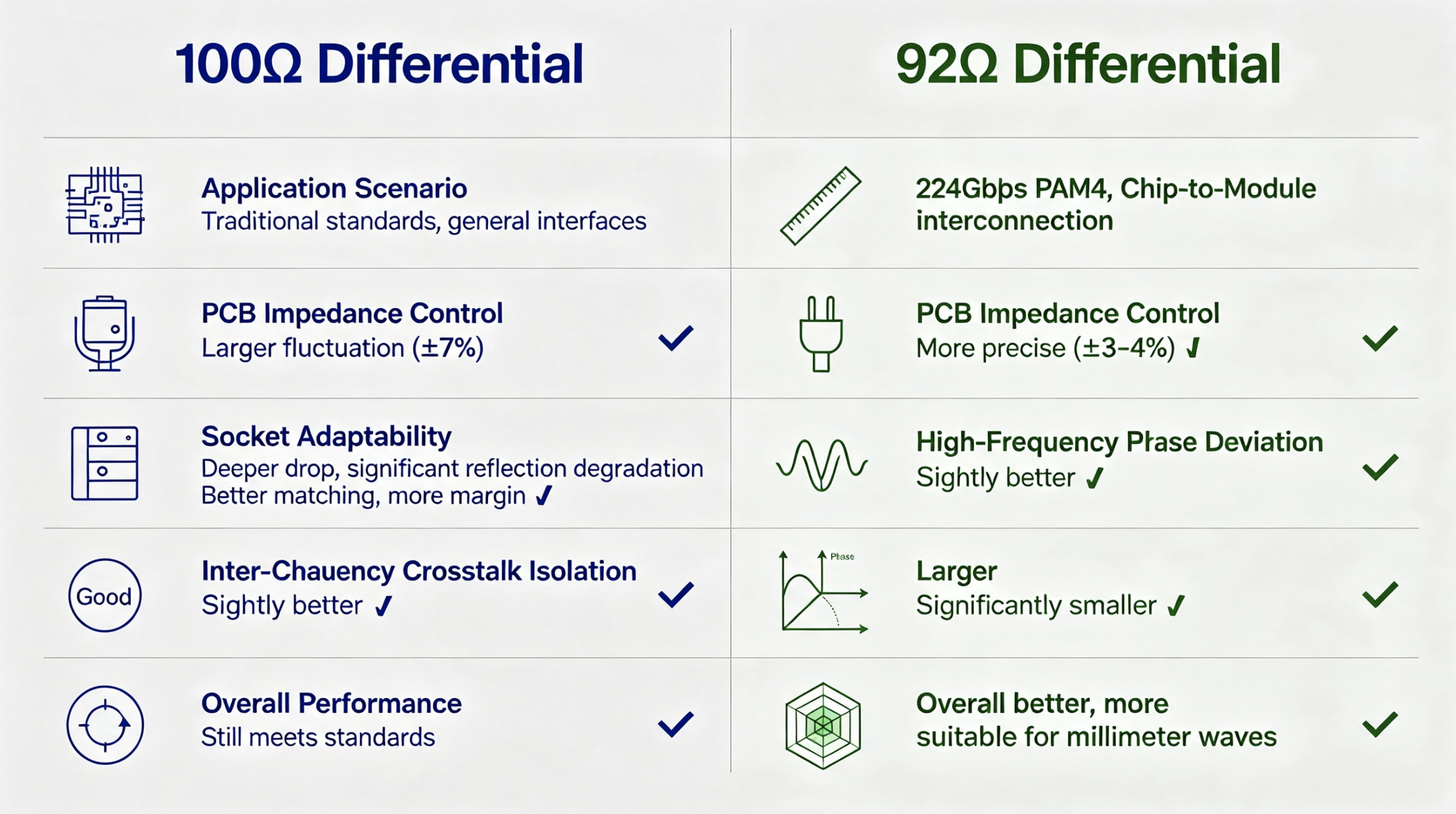
The industry's technical direction is becoming clear: IEEE 802.3dj and OIF discussions around 224Gbps PAM4 C2M (Chip-to-Module) interconnects are trending away from the traditional 100Ω differential impedance, toward 92Ω — an impedance that sits closer to the real electrical behavior of sockets and connectors. 92Ω means less reflection and more margin; it's the native impedance for mmWave, not a downgraded version of a legacy 100Ω design.
But in practice, most test interface suppliers either grind away on a single 100Ω spec, or spin an entirely new PCB to support 92Ω — same chip, two boards, double the cost, double the schedule.
Our answer: the same PCB design, validated for both 100Ω and 92Ω in a single simulation pass — not a compromised "compatibility" fallback, but native dual-impedance design capability. The data backs up why 92Ω genuinely fits mmWave better: phase deviation across the 8-lane bus measured just 0.35° at 92Ω, versus 4.52° at 100Ω — more than an order of magnitude difference. Return loss degradation after the socket is introduced was also meaningfully more contained at 92Ω.
This isn't just a simulation report. It's a call worth the industry taking seriously: at 224Gbps mmWave speeds, 92Ω may be the choice that's actually built for what's coming next.
Point Two: "Once you're at mmWave, the socket isn't a negligible mechanical part anymore"
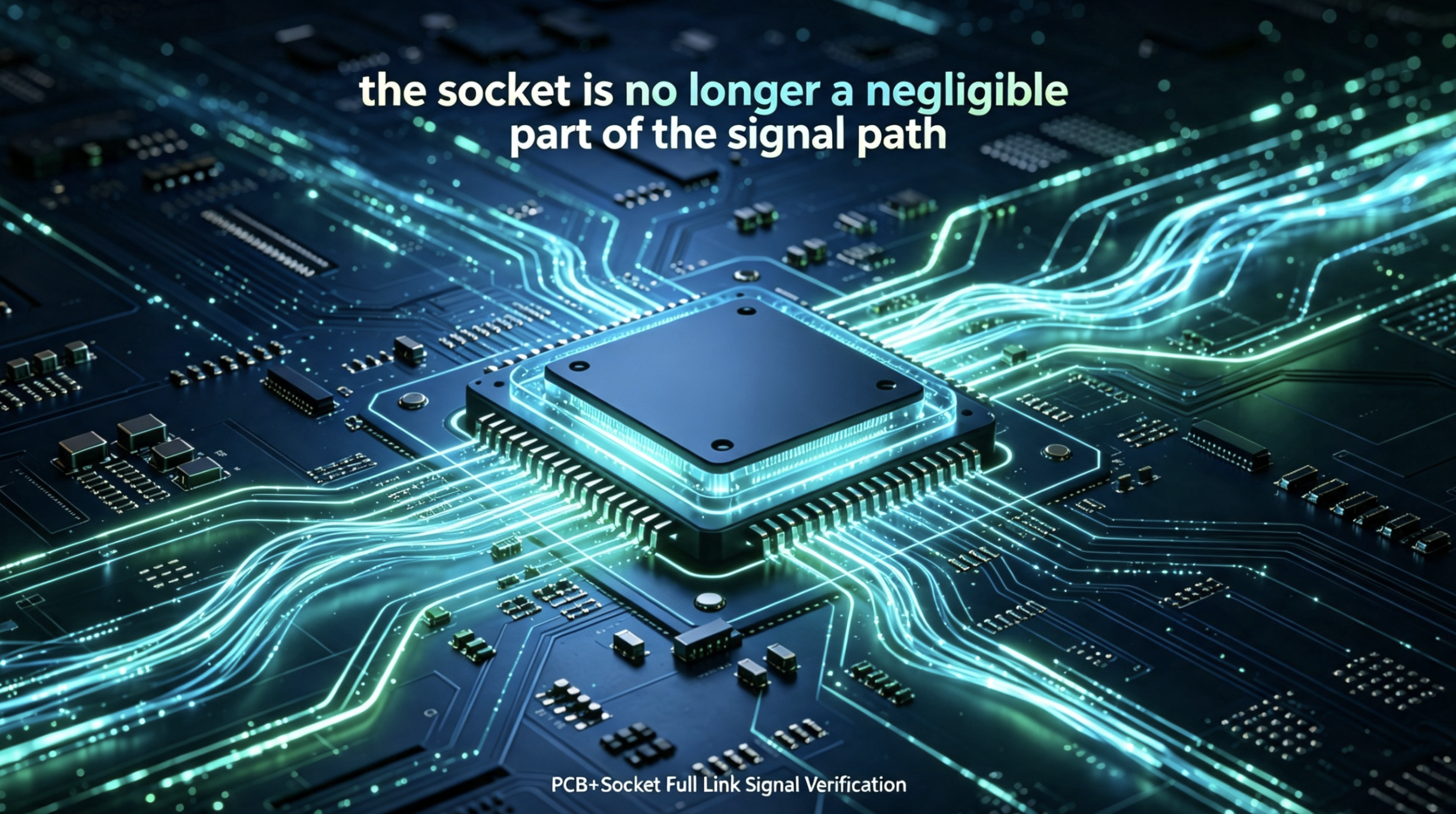
Almost every team running SI simulation unconsciously treats the socket as an "ideal connector" — simulate the PCB, build the sample, watch it fail real-world testing, then start a guessing game to find the problem. That blind spot didn't matter much at lower speeds. At mmWave frequencies, socket-induced impedance drop is now substantial enough to be the single biggest variable in system performance.
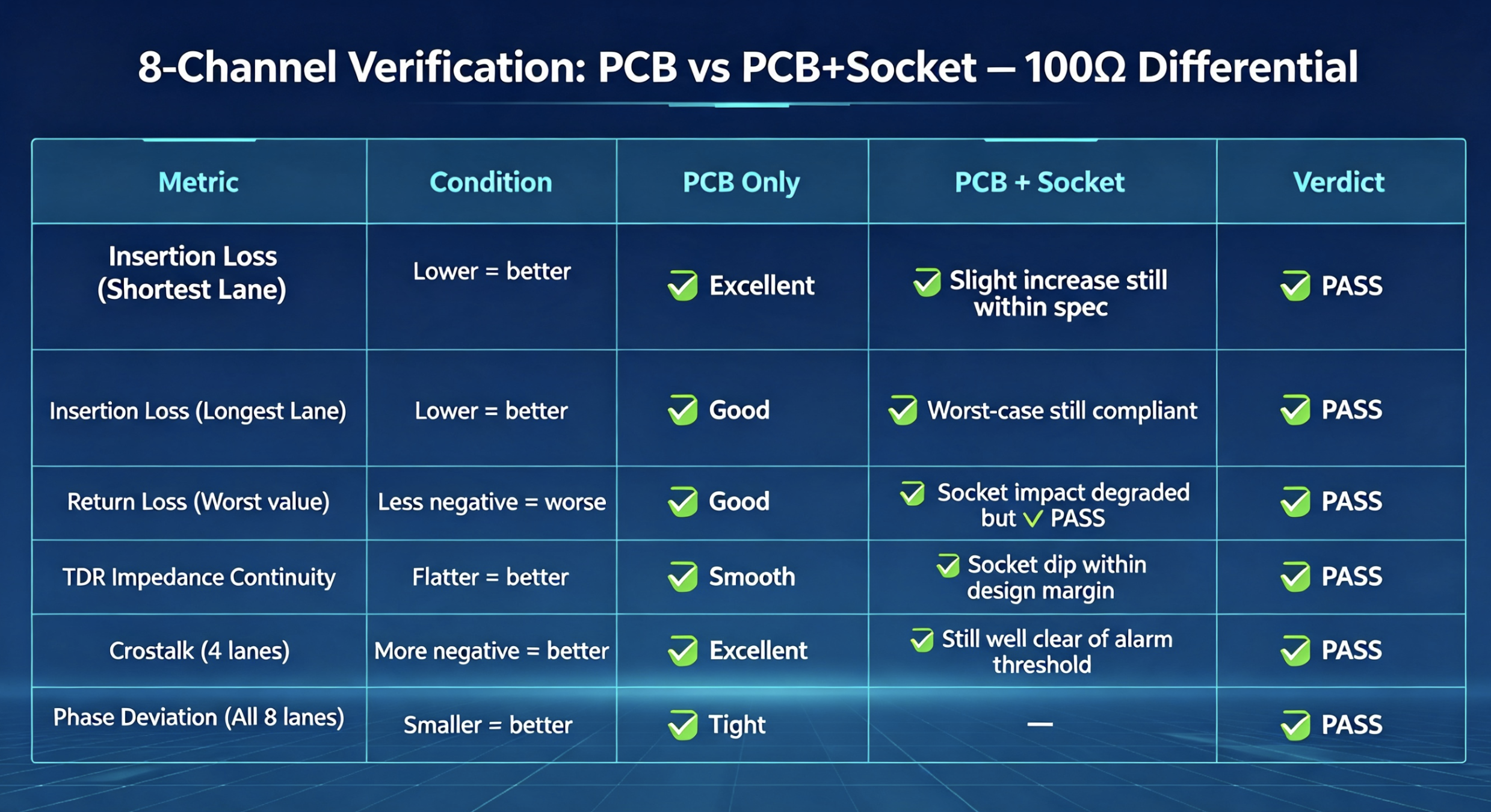
Our validation data puts a number on this "invisible bottleneck": introducing the socket degrades insertion loss by 0.3–0.5dB and drops return loss by 3–5dB — the TDR impedance curve can fall from an ideal ~100Ω range down to roughly 82Ω, and from an ideal ~92Ω range down to roughly 77Ω. That's not noise you can round away — it's a real, systematic variable that can absolutely be accounted for at the design stage.
Our approach is direct: build the socket into the same simulation loop, instead of discovering the problem after the sample is built. Using a full PCB+Socket co-simulation methodology on the HFSS platform, we predict socket-induced loss and reflection at the design stage and build in margin ahead of time — the result: every configuration, PCB-only or PCB+Socket, PASS.
Once you're at mmWave speeds, the socket isn't a mechanical afterthought anymore — it's the single largest source of impedance drop in the signal path. Does your simulation account for it?
Point Three: "Showing only your best-case lane isn't credibility"
Here's another industry open secret: most simulation decks quietly show only the shortest, best-performing lane — and skip the longest lane, where routing margin is tightest. The result shows up later: inconsistent yield in production, problems that don't reproduce — because the real bottleneck was never actually validated in the first place.
We do the opposite: both the shortest and longest lanes across an 8-lane bus, validated independently and completely — insertion loss, return loss, TDR, crosstalk, and phase, all five key metrics, under the worst-case routing condition, all PASS. At the same time, we validated both major socket technology families — elastomer and pogo-pin — in parallel, so customers keep real flexibility in socket selection without needing a redesign.
Showing only your best-case lane was never a source of credibility. Every lane meeting spec at the worst-case condition — that's a real production-scale promise.
What This Means for Customers
224Gbps shouldn't be an isolated PCB-level metric. It should be a system-level commitment that holds up under three tests:
is the impedance target aligned with where the industry is actually heading,
is a "hidden variable" like the socket genuinely built into validation,
and does the entire bus still hold up under worst-case conditions.
These three fronts are exactly where SEMIROC keeps investing in ultra-high-speed interconnect validation — and where we think the rest of the industry needs to catch up.
About SEMIROC
SEMIROC is a one-stop solutions provider for ATE interface hardware, covering DIB, PIB, Probe Cards, MLO substrates, and cable assemblies, with full-chain capability from system-level signal/power integrity simulation and high-density routing optimization to large-panel mechanical reliability design. SEMIROC serves leading semiconductor manufacturers and test partners worldwide.
Contact our customer service team now to find answers to your questions.
CONTACT US