Layer Efficiency and Mechanical Reliability for High Site-Count MAP Test —— Semiroc Case Study5


When "Cost Efficiency" and "High-Density Parallel Test" Both Have to Hold True
An Industry Trend Driven by Cost Pressure
Mobile SoC is one of the rare chip categories where test scale and cost sensitivity are both pushed to the extreme at the same time: shipment volumes run into the hundreds of millions, production cycles are tight, and the window for NPI (New Product Introduction) is often measured in weeks. That combination pushes the entire industry in one direction — run MAP (Multi-site Array Package) test at the highest practical site count, while driving test interface hardware manufacturing cost as low as possible.
These two goals naturally pull against each other. More sites means tighter routing and a higher risk of signal-power interference, which typically calls for more PCB layers to route everything cleanly — and more layers means higher cost and greater yield risk. Whether a supplier can deliver the same, or better, electrical performance with fewer layers is becoming a real benchmark for engineering capability in this space. A recent high site-count mobile SoC MAP test project we worked on is a direct case study in exactly this trade-off.
The Typical Challenges in This Class of Project
Take a recent high-pin-count mobile SoC MAP test project we worked on as an example (specific customer details have been anonymized per confidentiality requirements). The project's defining characteristics were:
- Device pitch in the 0.35mm fine-pitch range, with parallel site count reaching double digits, over 1,300 pins per site, and a substantial combined signal/power net count once all sites were aggregated
- Per-site DUT current demand in the tens-of-amps range, with signal-power interference risk rising sharply once multiple sites ran simultaneously
- Two core risks stood out: ① contact stability degradation at outer sites as routing became more congested; ② signal-power interaction caused by high-density routing
On the fabrication side, projects of this class typically require PCB layer counts approaching 70 layers and large panel sizes approaching 20"x24" just to accommodate this density of nets. But a large panel introduces its own mechanical risk — BGA pad positioning further from the panel center is more exposed to overall panel tolerance, and that challenge is amplified further by the layout demands of densely packed components like relays, MOSFETs, and high-speed switches.
SEMIROC's Design Methodology: Doing More With Fewer Layers
Methodology 1: System-Level Electrical Simulation
For long-channel high-speed interfaces, we run full signal integrity (SI) simulation and verify power target impedance and ripple — evaluated at the system level across the entire panel, not in isolation site by site.
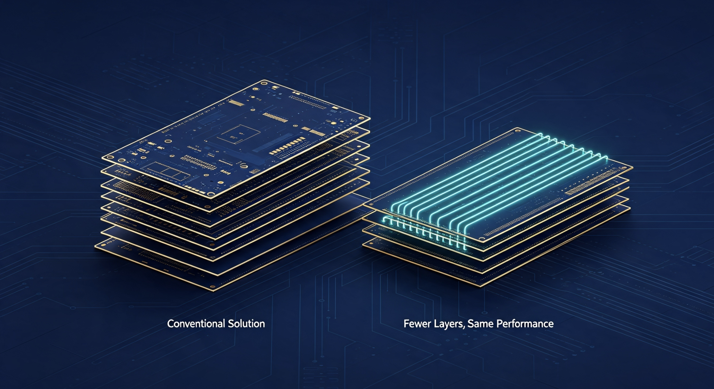
Methodology 2: Layer-Constrained Routing Optimization — Roughly 20% Fewer PCB Layers Than a Comparable Approach
This is the point worth dwelling on: while meeting the same electrical performance targets, more refined routing strategy and stack-up planning allowed us to deliver the final design using roughly 20% fewer PCB layers than a typical competitor approach. This isn't a spec cutback — it's achieving the same performance target through more efficient routing topology under a heavily constrained signal/power net density, translating directly into a manufacturing cost advantage customers can actually feel.
Methodology 3: PDN Optimization for Dense Switching Elements
Relays, MOSFETs, and other high-speed switching components packed densely together place additional transient load stress on the power distribution network (PDN). We built targeted PDN optimization to keep power ripple under control even in dense switching scenarios.
Methodology 4: Mechanical Reliability Design for Large Panels
For the alignment challenges of large panels and far-edge BGA pads, panel-wide tolerance and long-term reliability were built into the design from the outset — rather than being addressed reactively once warpage or misalignment shows up in production.
Methodology 5: DFM Tailored for High-Density Structures
The overall design fully accounts for manufacturability requirements under high component density and structural complexity, ensuring the design isn't just simulation-compliant, but stable in actual volume production.

What This Means for Customers
For a cost-sensitive, high-volume category like mobile SoC, the value of test interface hardware isn't just "can it test the part" — it's delivering on three fronts at once:
- Manufacturing cost: fewer PCB layers translate directly into lower manufacturing cost and shorter lead times — an advantage that compounds into real savings on programs shipping in the millions of units;
- Test stability: solid outer-site contact stability and signal/power isolation means yield consistency holds up even at high parallel site counts;
- Production reliability: building large-panel mechanical tolerance into the design from the start reduces rework and yield loss caused by warpage or misalignment once in volume production.
This is exactly the direction SEMIROC keeps refining in high-density MAP test — not treating electrical performance and cost as opposing forces, but using stronger simulation and routing engineering capability so customers don't have to choose between testing it well and being able to afford it.
About SEMIROC
SEMIROC is a one-stop solutions provider for ATE interface hardware, covering DIB, PIB, Probe Cards, MLO substrates, and cable assemblies, with full-chain capability from system-level signal/power integrity simulation and high-density routing optimization to large-panel mechanical reliability design. SEMIROC serves leading semiconductor manufacturers and test partners worldwide.
Contact our customer service team now to find answers to your questions.
CONTACT US