Signal Integrity Design for 224Gbps mmWave Test —— Semiroc Case Study4


When Signal Speed Enters mmWave Territory, the Via Becomes the Weak Link
An Industry Trend That's Accelerating
Whether it's high-speed interconnects for AI accelerators or next-generation high-performance computing chips, signal speeds are racing toward the 224Gbps mmWave range at a visible pace. This speed range has moved beyond the experience base of conventional digital circuit design — at this frequency, any small geometric discontinuity leaves a clearly visible scar on the signal path.
Test interface hardware is precisely the link in that signal path that's easiest to overlook — and most consequential. A recent mmWave high-frequency test project we worked on confirmed exactly this: once signal speed enters the 224Gbps range, via impedance discontinuity becomes the primary source of insertion loss and return loss degradation across the entire test system. This article breaks down the technical logic behind it.
The Typical Challenges in This Class of Project
Take a recent mmWave device test project we worked on as an example (specific customer details have been anonymized per confidentiality requirements). The project's defining characteristics were:
- Built on a high-end mmWave-class tester platform, using a vertical probe architecture, covering full high/low temperature range testing
- Device pad size in the sub-millimeter range, with each site carrying hundreds of signal channels alongside a substantial overall current demand
- The core risk was concentrated in via impedance discontinuity, directly affecting insertion loss and return loss performance at 224Gbps
At mmWave frequencies, the conventional design sequence of "get current and signal routed first, optimize impedance later" no longer holds up. The reason is straightforward: at this frequency range, impedance discontinuity isn't just a "signal quality" issue anymore — it's a "whether the signal transmits correctly at all" issue. Even a minor resonance caused by via stubs can significantly degrade the entire link's high-frequency performance.
On the fabrication side, projects of this class typically call on process specs near the top of SEMIROC's platform capability — PCB layer counts reaching the 100+ tier and MLO substrates built on advanced high-layer stack-ups — along with stringent plating thickness uniformity requirements, because minor plating thickness variation translates directly into impedance shift and resonance risk, the central trade-off on the fabrication side of any mmWave project.
SEMIROC's Design Methodology: Treating Impedance as the First Variable
Methodology 1: 3D Electromagnetic Modeling
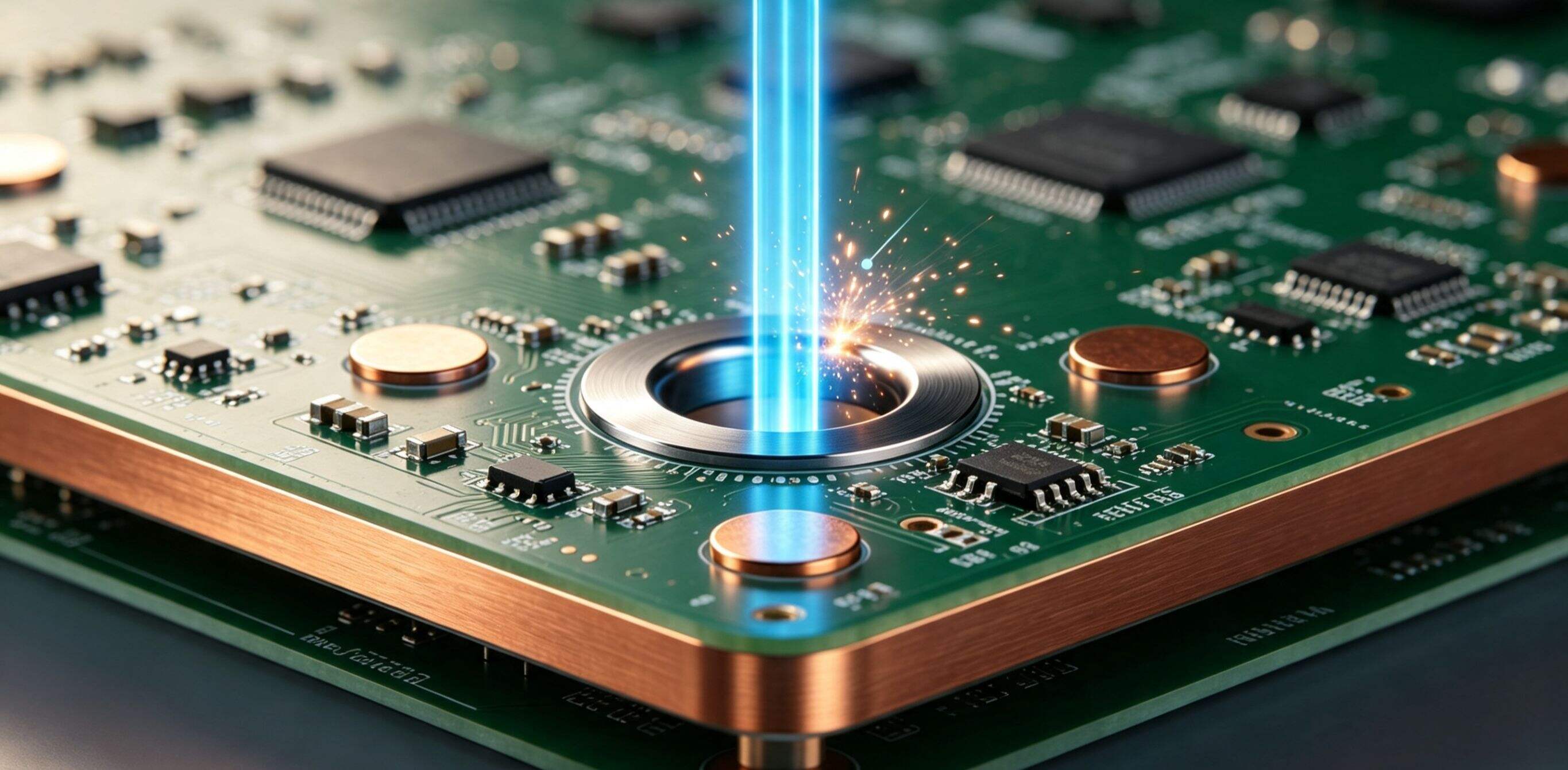
At mmWave frequencies, conventional 2D transmission line models can no longer accurately predict the electrical behavior at via and pad transition regions. We run full 3D electromagnetic (EM) simulation on every critical via and pad transition structure, identifying geometries that could trigger resonance or loss degradation before sample testing — not after.
Methodology 2: Fine-Grained Impedance Control
mmWave signals have extremely low tolerance for impedance deviation. Through strict process control over pad opening size and plating thickness, we hold overall impedance within a tight target range (±7%), and actively suppress via stub resonance through optimized via geometry — a key precondition for meeting 224Gbps insertion loss targets.
Methodology 3: Surface Finish and Loss Mitigation
At this frequency range, copper surface roughness becomes a significant loss variable. Our material selection and process control account for surface roughness and barrel plating uniformity together, turning "invisible" manufacturing details into measurable high-frequency performance.
Methodology 4: Probe Co-Design for RF Contact Consistency
High-frequency testing demands far greater probe contact consistency than conventional digital testing. We optimize landing pad-to-probe-needle matching specifically to ensure RF signal contact repeatability, while tightly controlling scrub/overdrive amplitude to avoid damaging the RF contact surface. Surface finish specifications are derived directly from 224Gbps tolerance requirements, and the alignment fiducial scheme is specifically calibrated for large-area probe arrays to ensure RF consistency across the array. Even after needle replacement, clearly defined tolerances prevent RF performance degradation.

What This Means for Customers
mmWave-class signal speeds are shifting from "cutting-edge" to "production requirement," and this shift raises the bar for test interface hardware suppliers in two ways:
- Getting the "invisible" details right — like via structures directly determines whether insertion loss and return loss meet the specifications customers ultimately sign off on;
- Controlling minor manufacturing variation — plating thickness, surface roughness — determines consistency and yield at volume, not just performance on a lab sample.
That's why SEMIROC continues to invest in high-speed signal simulation and advanced MLO manufacturing capability — from 224Gbps ultra-high-speed signal design capability to RF contact consistency at the probe level. As signal speeds keep climbing, we want to make sure test interface hardware is never the bottleneck holding customers back.
About SEMIROC
SEMIROC is a one-stop solutions provider for ATE interface hardware, covering DIB, PIB, Probe Cards, MLO substrates, and cable assemblies, with 224Gbps ultra-high-speed signal design capability. PCB layer count capability reaches the 100+ tier, and MLO substrates support advanced stack-up structures. SEMIROC serves leading semiconductor manufacturers and test partners worldwide.
Contact our customer service team now to find answers to your questions.
CONTACT US