Power Integrity Design for High-Density Multi-Site Parallel Test | Semiroc Case Study 3


When "Site Count" — Not "Per-Site Current" — Becomes the First Design Variable
An Industry Trend Already Underway
Rising test cost pressure on AI and high-performance chips is pushing the entire industry in the same direction: pack as many parallel test sites as possible into a single test cycle, spreading per-unit cost across a larger batch. This shift is especially visible in digital device and AI chip testing — what used to be a dozen-or-so parallel sites is increasingly giving way to test schemes running thirty, forty, or more sites in parallel as a standard configuration for high-end digital chips.
But this trend brings a design challenge that's easy to underestimate: once site count climbs high enough, the real ceiling on design usually isn't signal integrity (SI) anymore — it's power integrity (PI). A single site's current draw may not be extreme on its own, but when dozens of sites pull current from the same power network simultaneously, cumulative current across sites erodes the power system's design margin fast. This is exactly the conclusion we validated on a recent high-density parallel test project, and it's the technical story this article unpacks.

The Typical Challenges in This Class of Project
Take a recent high-pin-count digital / AI chip parallel test project we worked on as an example (specific customer details have been anonymized per confidentiality requirements). The project's defining characteristics were:
- 30+ sites running simultaneously, using a vertical probe architecture, covering full high/low temperature range testing
- Each site carried hundreds of signal and power channels — per-site current demand wasn't extreme on its own, but the cumulative current across all sites running at full load was substantial
- Device pad size and pitch were already in the sub-100µm fine-pitch range, placing higher demands on probe contact stability
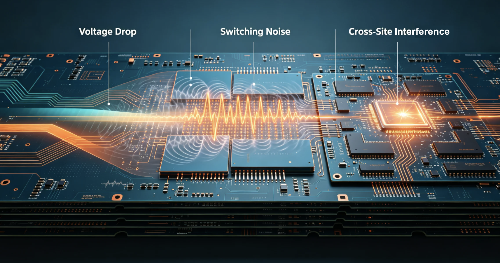
In projects like this, the power network design faces three escalating risks:
- Voltage drop: actual voltage delivered to the chip deviates from the target, directly distorting test results;
- Power noise: switching noise from high-speed switching activity interferes with accurate high-speed digital signal reads;
- Cross-site interference: without properly zoned power planes, current fluctuation at one site can propagate and destabilize voltage at neighboring sites — and the larger the parallel site count, the more amplified this chain-reaction risk becomes.
On the fabrication side, projects of this scale typically call on process specs near the top of SEMIROC's platform capability — PCB layer counts reaching the 100+ tier and MLO substrates built on a 15+20+15 advanced stack-up — to satisfy dense power zoning and high-speed signal integrity simultaneously within limited board real estate. This is precisely why we continue to invest in high-layer-count, high-density MLO manufacturing capability.
Our Design Methodology: Putting Power First
Methodology 0: PI Pre-Simulation Technology
Modeling and simulating the Power Delivery Network (PDN) prior to the design phase focuses on verifying power module load capability, ripple noise, and transient response, as well as evaluating the impact of PCB parasitic parameters on power quality. This approach identifies power integrity risks early, optimizes component selection, decoupling networks, and stackup design—thereby reducing prototype iterations and effectively lowering development costs. Pre-simulation ensures a stable and clean power supply foundation before volume production, providing robust support for high reliability and high-precision ATE test boards.
Methodology 1: PI-Driven Design Flow
Unlike the conventional approach of "route signals first, add power later," in high-site-count parallel test scenarios we take a power-first design approach: complete power network zoning and routing before signal design begins, then design signals within that established power constraint. The logic is straightforward — when power is the true design ceiling, signal integrity issues can typically be resolved effectively once power is stable; the reverse rarely holds.
Methodology 2: Large-Scale Power Simulation
The design phase runs three categories of simulation validation to ensure the solution holds up under full-load conditions:
- Power Integrity (PI) Simulation: Evaluates impedance performance under multi-site full-load conditions to strictly maintain it within the target impedance profile.
- Current Distribution Analysis: Identifies and eliminates localized current hotspots in advance.
- IR Drop Analysis: Verifies stable voltage supply across all sites under maximum load conditions.
- Stackup Design Optimization
- Decoupling Capacitor Network Optimization
- Fan-Out Via Optimization
Methodology 3: Site Power Isolation Design
Using power plane zoning and stitching techniques, we optimize return current paths and keep each site's power domain as independent as possible — structurally blocking the chain reaction where one site's current fluctuation destabilizes its neighbors. This isolation logic extends into the probe-side co-design as well: landing pad-to-probe-needle matching and scrub/overdrive tuning are both specifically optimized against PI-induced variation, ensuring contact impedance doesn't drift over extended volume testing.
What This Means for Customers
High-density parallel testing is becoming the industry norm — but whether power integrity is genuinely engineered right directly determines two outcomes customers care about most:
- Stable test results: a properly designed power network means every site gets its target voltage under full-load current, fundamentally reducing false failures caused by voltage drop or noise, and protecting First Pass Yield (FPY);
- Predictable yield: zoned power isolation reduces cross-site interference risk, making volume test yield more predictable and preventing isolated site anomalies from dragging down overall output.
As the industry continues moving toward higher site counts and greater parallelism, power integrity design capability is becoming the real benchmark for whether a test interface hardware supplier can genuinely deliver on high-end programs. That's why SEMIROC keeps investing in simulation-driven design platforms and refining our joint PI/SI design capability — so customers don't have to trade test cost against test reliability as they scale.
About SEMIROC
SEMIROC is a one-stop solutions provider for ATE (Automated Test Equipment) interface hardware, covering DIB, PIB, Probe Cards, MLO substrates, and cable assemblies, with full-chain capability from high-speed signal simulation and high-current/multi-site power integrity design through to volume delivery. PCB layer count capability reaches the 100+ tier, and MLO substrates support advanced 15+20+15 stack-ups. SEMIROC serves leading semiconductor manufacturers and test partners worldwide.
Contact our customer service team now to find answers to your questions.
CONTACT US