Case Study 2: 50GHz High-Frequency & 54,000-Pin Extreme Density — Semiroc Overcomes Barriers in AI Mixed-Signal Chip Testing


Industry Trends: High-Frequency and High-Power as the "Dual Pressure" on Advanced Packaging
In the 2026 era of AI and High-Performance Computing (HPC), integrated circuits are evolving beyond mere physical scaling toward higher-frequency, higher-power Mixed-Signal architectures. As signal rates surge to the 50GHz level and individual chip pin density explodes exponentially, test interfaces often face the ultimate dual test of electromagnetic integrity and mechanical stress. No matter how perfect the chip design is, if a stable and consistent test environment cannot be provided during mass production, high-yield mass production remains unattainable.
Project Background and Core Challenges
This project focuses on wafer-level vertical probe testing for a next-generation high-end AI/Mixed-Signal chip, utilizing the industry-leading Teradyne UltraFLEXplus (UF+) test platform. Although this project adopts a Dual-Site layout, its design complexity and manufacturing difficulty represent an industry "ceiling":
- 50GHz Ultra-High-Frequency Signal Transmission: At the 50GHz band, signal attenuation and crosstalk are extreme, requiring the interface network to meet rigorous multi-impedance matching standards (covering 50Ω/80Ω/90Ω/100Ω).
- Staggering 54,000+ Pin Density: With 27,367 pins per site, the total pin count exceeds 54,000. Such large-scale probe integration poses immense challenges for overall downward pressure uniformity, coplanarity, and thermal management.
- High-Density, High-Current PI Crisis: Each site carries up to 60 independent Power Rails. The PDN (Power Delivery Network) under continuous high-density current is highly susceptible to degradation, risking severe contact instability.
Fig 3: High-Current Surface Finish Comparison
The left side illustrates the ablation risk of traditional solutions under frequent overloads, while the right side presents the zero-wear contact effect achieved by Semiroc’s proprietary material modification. Through needle geometry matching and surface treatment, long-term stability is achieved throughout the testing cycle.
(Note: Numerical variables in the test comparison curve are desensitized placeholders; actual metrics are protected by customer NDA.)
Our Solutions
1. Architectural Breakthrough: 68-Layer M6 PCB and 10+16+10 MLO Architecture
To smoothly manage 60 power rails and over 1,300 high-speed signal lines within an extremely confined space, Semiroc pushed manufacturing limits by adopting a 68-layer M6 high-Tg PCB integrated with a 10+16+10 MLO (Multi-Layer Organic) vertical stack-up.
- Multi-layer Shielding and Lossless Transmission: The 68-layer design provides superior inter-layer shielding. Combined with the 10+16+10 MLO substrate, it completes complex signal transitions within an ultra-short physical path, minimizing internal insertion loss and parasitic effects for 50GHz signals.
- Precision Impedance Control: By optimizing via geometry, multi-stream composite impedance accuracy is strictly maintained within ±7%.
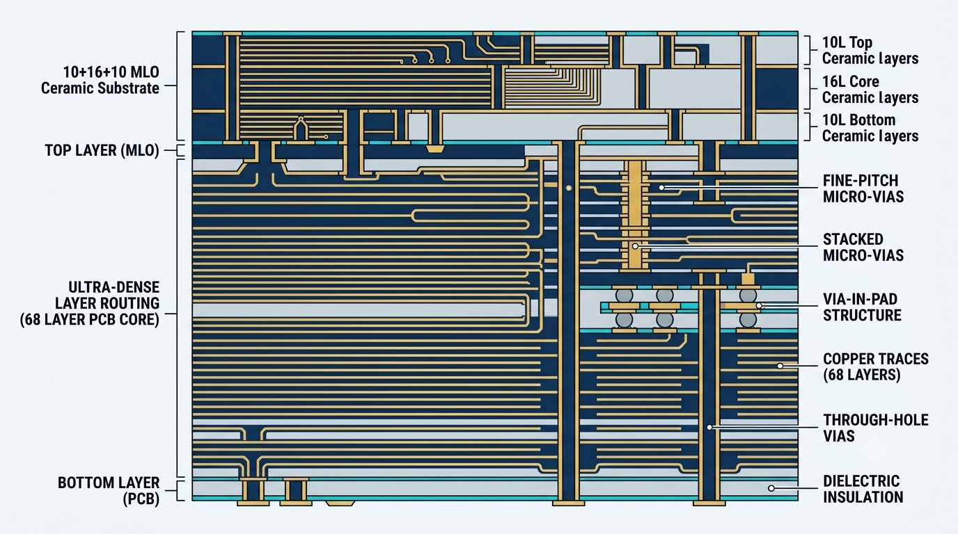
Fig 2: Schematic of the 68-layer M6 ultra-high layer count PCB and 10+16+10 MLO vertical stack-up architecture.
This illustration demonstrates the architectural logic for achieving high-performance multi-layer transition within an extremely confined physical space, utilizing high-density micro-vias and precision inter-layer routing to meet the requirements for efficient 50GHz high-frequency signal transmission.
(Note: Special process and layer stacking parameters have been desensitized; provided for architectural logic and routing path illustration only.)
2. Innovative Routing: Resolve PDN Congestion
In traditional routing logic, thousands of high-current probes rapidly saturate metal planes, triggering severe PDN congestion.
- Full Blind/Buried Via Synergy: Semiroc introduces a multi-level combination topology utilizing Via-in-pad combined with PTH (Plated Through-Hole) and BVH (Blind/Buried Via Hole) technologies.
- Power Plane Partitioning: The simulation team has defined physically isolated power planes for each test site, optimized IR drop and AC impedance, fundamentally eliminating power transient interference and noise coupling caused by sudden high currents during multi-site parallel testing.
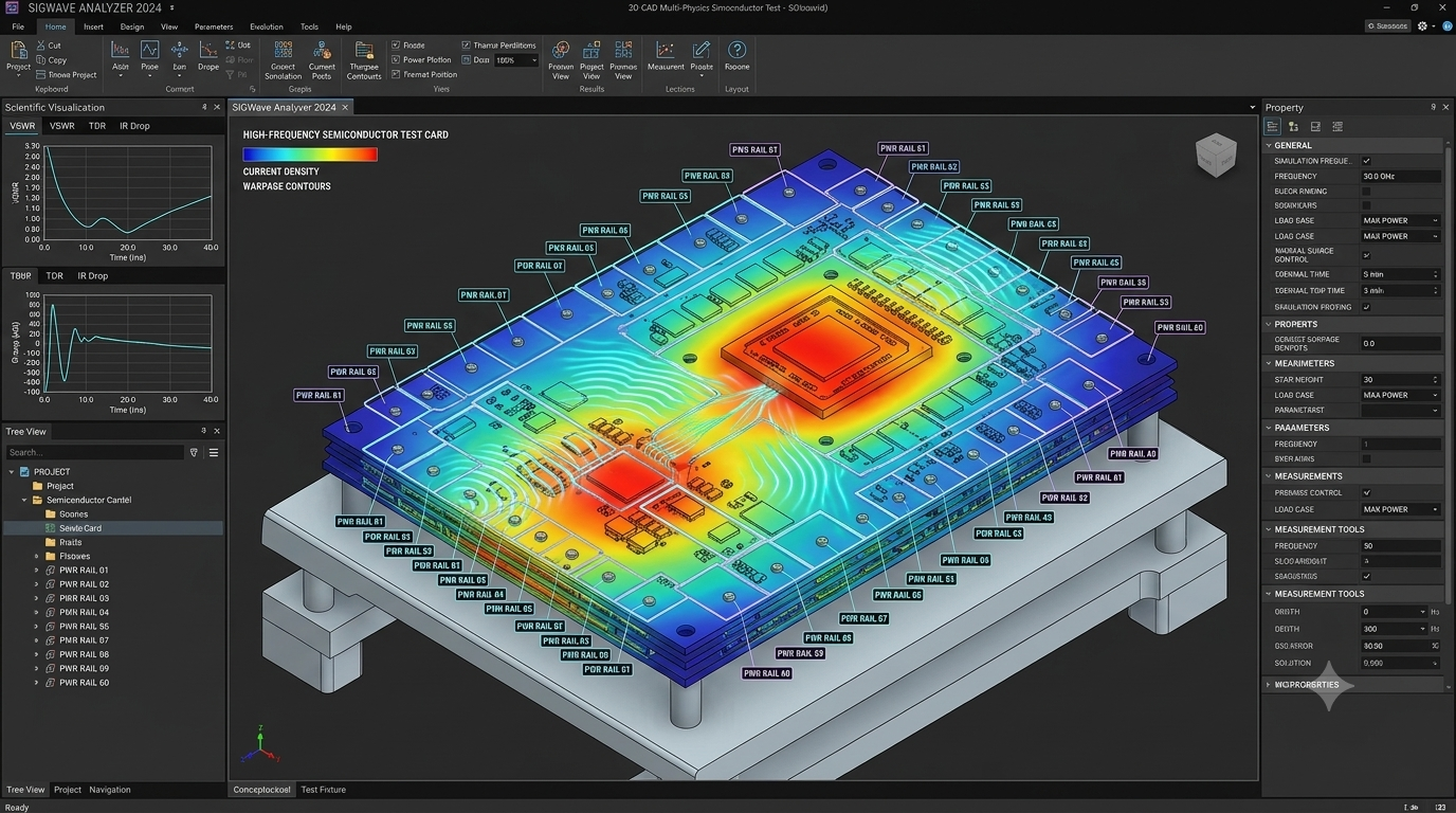
Fig 3: Multi-physics coupling simulation analysis of 50GHz high-speed signal topology and 60-rail PDN independent plane partitioning.
Through thermal distribution and electromagnetic coupling analysis, this visualization intuitively presents the design logic of utilizing physical partitioning to effectively suppress transient interference and power noise coupling in Dual-site parallel testing mode.
(Note: Frequency domain and current density cloud map data are desensitized illustrations under typical high-frequency operating conditions.)
3. High-Current Surface Finish and Needle Matching: Eliminating Contact Instability
In high-current probing, the microscopic contact interface between the needle tip and the pad is highly susceptible to "micro-arcing" ablation or high-heat oxidation under frequent overloads.
- High-Current Dedicated Surface Finish: Semiroc has optimized material surface modification specifically for High-current Probing, ensuring the contact interface possesses high oxidation resistance and ultra-low, stable contact resistance (Cres).
- Precision Overtravel Control: Combined with deep Needle Shape Matching design and precision overtravel control, this effectively suppresses micro-contact instability. This not only protects high-value customer pads but also significantly extends the maintenance cycle of the probe card.
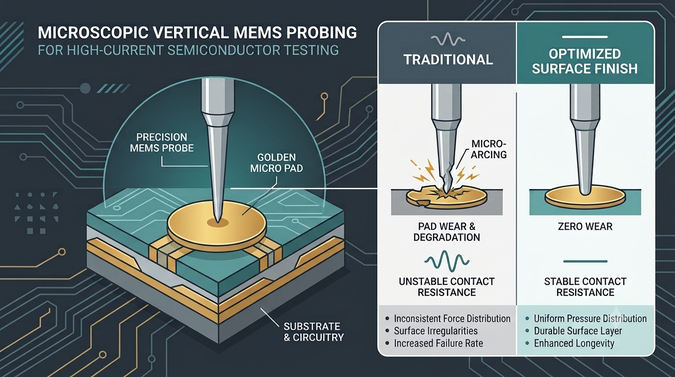
Fig 4: Comparison of surface finish optimization for high-current probing and microscopic contact resistance (Stable Cres) stability.
The left side illustrates the ablation risk of traditional solutions under frequent overloads, while the right side presents the zero-wear contact effect achieved by Semiroc’s proprietary material modification. Through needle geometry matching and surface treatment, long-term stability is achieved throughout the testing cycle.
(Note: Numerical variables in the test comparison curve are desensitized placeholders; actual metrics are protected by customer NDA.)
Why Choose SEMIROC?
In the fields of AI and HPC, 50GHz frequency and high-current stability are the two major hurdles for mass production yields. Through the successful delivery of this project, Semiroc has once again proven to the market: no matter how high your chip's power consumption is or how fast its signals are, we can provide a stable and consistent test environment.
- High-Frequency & High-Current Experts: One of the few global suppliers capable of mastering 50GHz high frequency, 60 power rails, and an extreme density of 54,000 pins simultaneously.
- Closed-Loop Engineering Excellence: Perfectly adapted to top-tier ATE platforms like Teradyne UF+, with a closed-loop supply chain spanning physical layer design, multi-dimensional simulation, and semiconductor-grade precision manufacturing.
- Guardians of Quality and Yield: We solve more than just PDN congestion and signal attenuation; we serve as the final line of defense for our customers' mass production success.
Contact our customer service team now to find answers to your questions.
CONTACT US