Case Study 1: Mastering Chiplet Probing: 120+ Site Parallel Testing
Industry Trend: Parallelism as the Strategic Edge in Advanced Packaging
As of 2026, the mass production efficiency of Chiplet architectures and HPC (High-Performance Computing) chips is defined by the test interface. With increasing die sizes and pin densities, the Cost of Test (CoT) has become a critical bottleneck. The industry demands interface solutions that can handle massive parallelism while maintaining extreme stability under wide temperature ranges.
Project Background & Core Challenges
This project involved wafer-level testing for a customer’s high-end AI ASIC. The device features an ultra-high pin count and is tested on the Teradyne UltraFLEXplus (UF+) platform.
- Massive Parallelism: Achieving over 120-site parallelism with over 20,000 high-performance vertical MEMS probes integrated into a single interface.
- Large-Area Probing: Managing mechanical pressure distribution and contact consistency for DUTs exceeding 100mm in size.
- Wide Temperature Range: Ensuring CTE (Coefficient of Thermal Expansion) matching across a rigorous -40°C to +150°C environment.
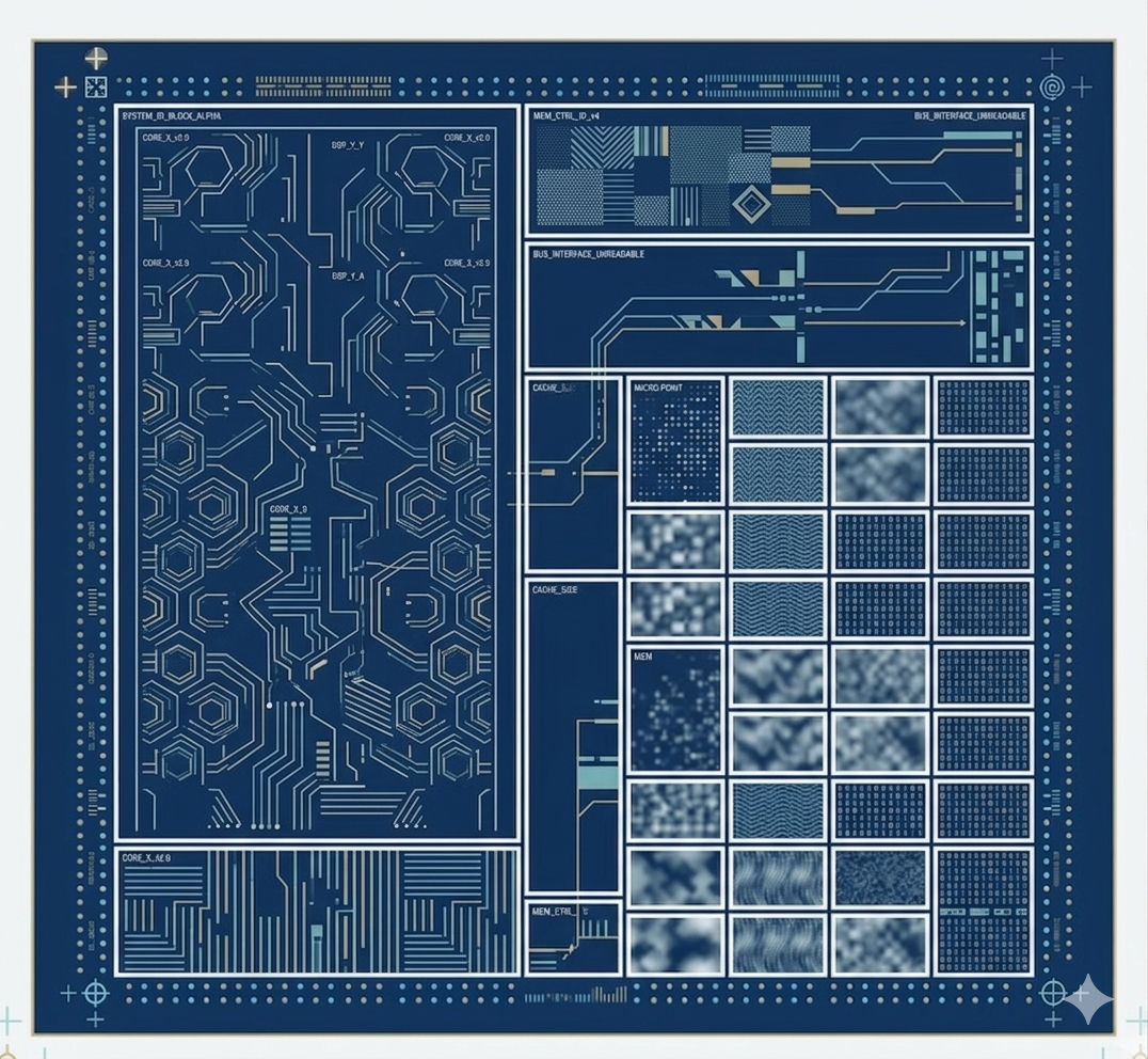
Project 1 High-Performance Computing Chip Detection Path Logic Abstraction Diagram (Anonymized)
Our Solutions
1. Advanced Fabrication: 50-Layer PCB & MLO Architecture
We utilized a state-of-the-art 50-layer high-Tg PCB coupled with a 5+2+5 MLO (Multi-Layer Ceramic/Organic) stack-up. Leveraging High-density Via-in-pad technology, we achieved precise routing for tens of thousands of signals within limited space, maintaining impedance at a strict 50Ω ±5%.
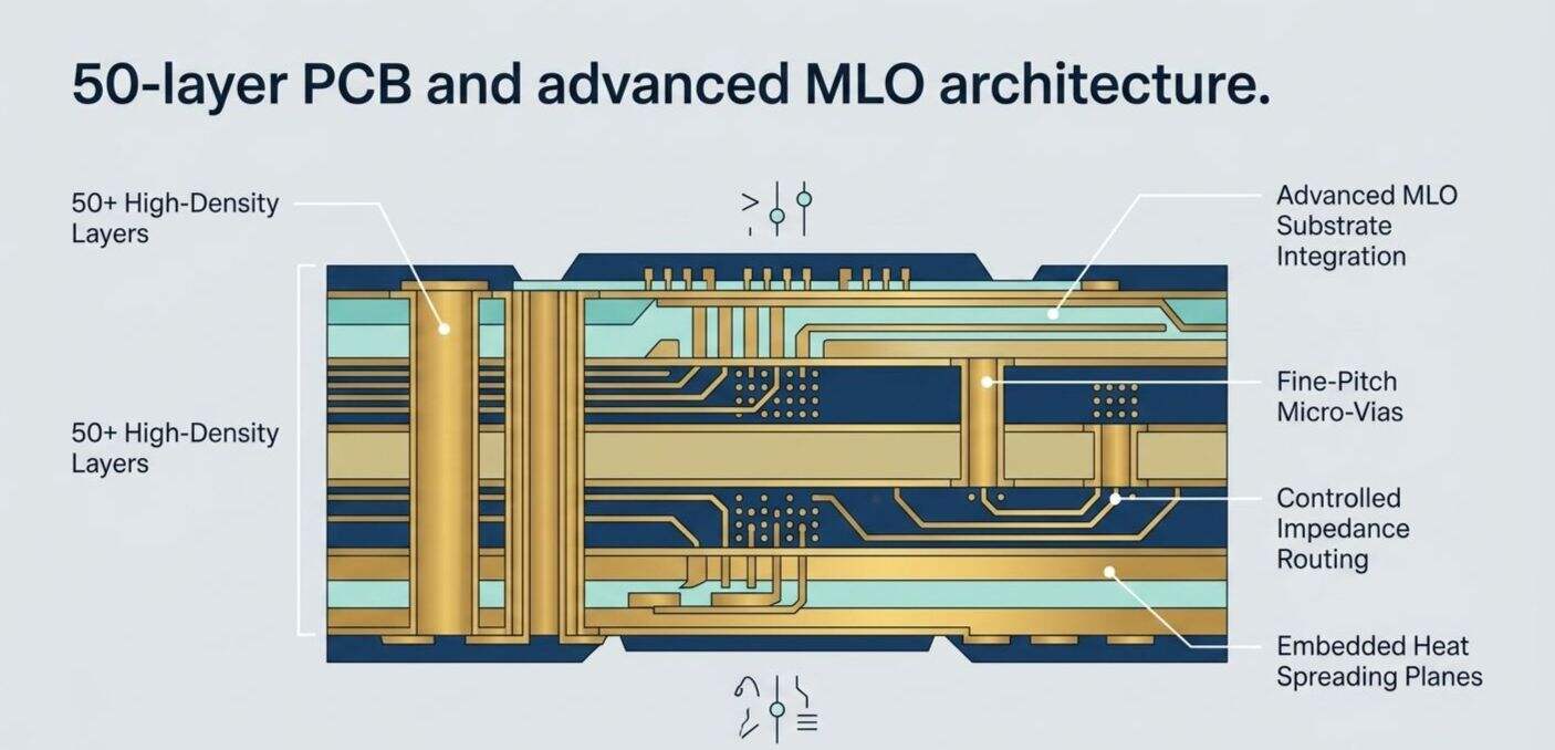
Fig 1: Cross-sectional schematic of Semiroc’s 50-layer ultra-high density PCB and advanced MLO substrate architecture.
(Note: Fabrication parameters are de-sensitized for confidentiality; for architectural illustration only.)
2. Multi-Physics Simulation & Stress Mitigation
By applying advanced Multi-physics Simulation, we performed Copper Balance Optimization across the PCB. This effectively mitigated warpage caused by thermal gradients, ensuring zero-miss probing even at the outermost sites.
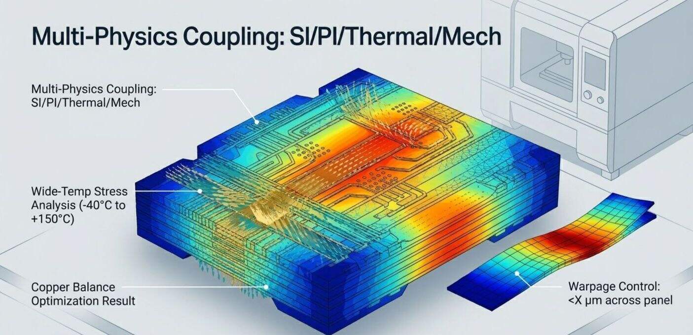
Fig 2: Multi-physics coupling simulation (SI/PI/Thermal/Mech) for vertical probing solutions under wide-temperature environments (-40°C to +150°C).
(Note: Simulation heatmaps represent de-sensitized data under typical operating conditions.)
3. Co-Design for Probe Longevity
Our Co-design services focus on micro-level contact precision:
- Needle Matching: Custom Needle Shape Matching tailored to the customer’s specific micro-pad geometries.
- Cost Efficiency: Precise Overdrive Control guarantees ultra-low contact resistance while minimizing pad wear, significantly extending probe card lifespan and reducing the overall Cost of Test.
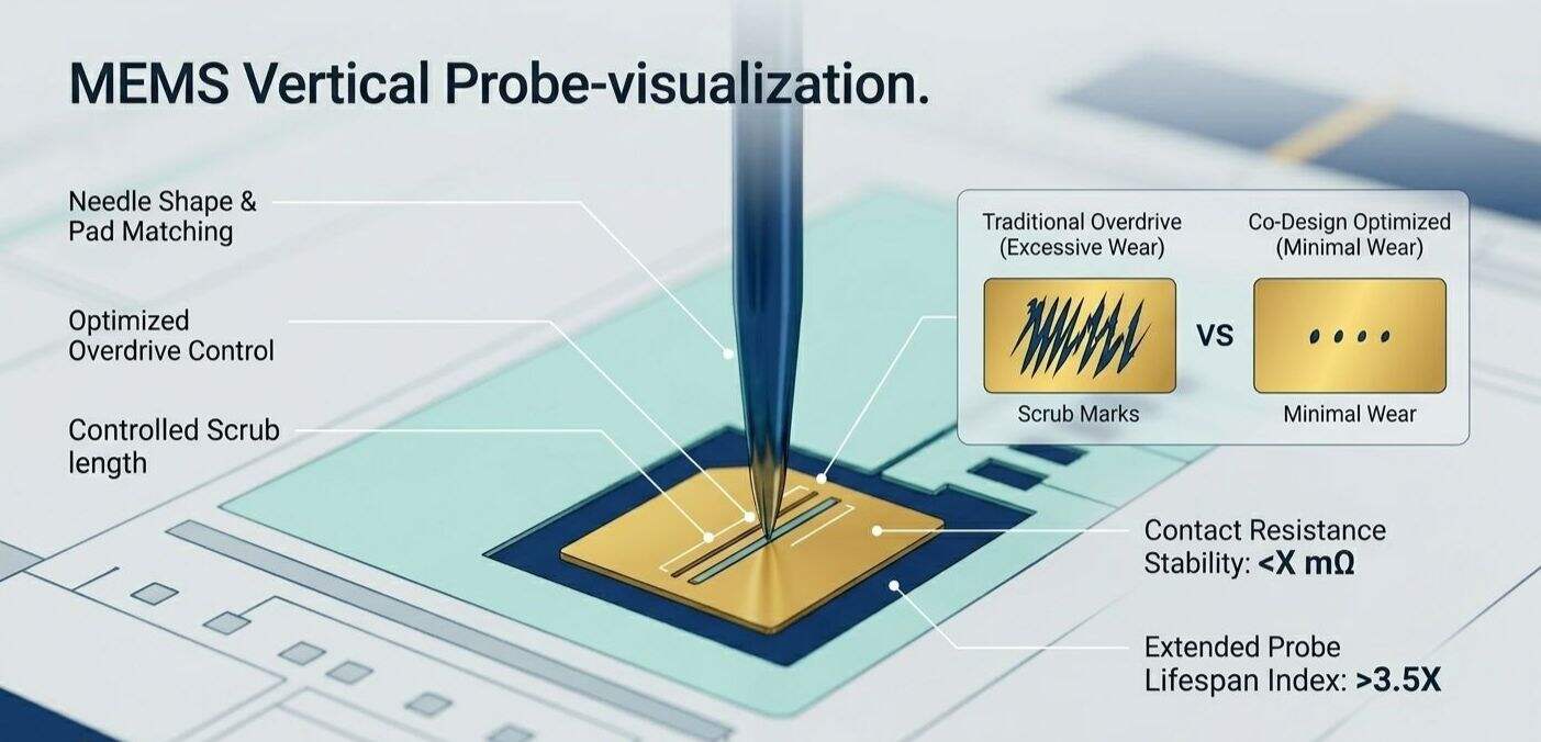
Fig 3: Micro-level comparison of scrub mark and pad wear optimized via Co-Design strategies.
(Note: Variable "X" serves as a de-sensitized placeholder; actual performance metrics are protected under specific testing NDAs.)
Why Choose Us?
- Proven Performance: One of the few global suppliers capable of delivering 120+ site massive parallelism solutions.
- System-Level Expertise: Seamless integration with leading ATE platforms like Teradyne UF+, offering end-to-end support from simulation to fabrication.
- Yield Enhancement: Beyond a simple interface, we empower high-value chip mass production through superior SI/PI design and reliability.
Contact our customer service team now to find answers to your questions.
CONTACT US