5 Common Errors in Semiconductor Burn-in Test Board Design and How to Avoid Them
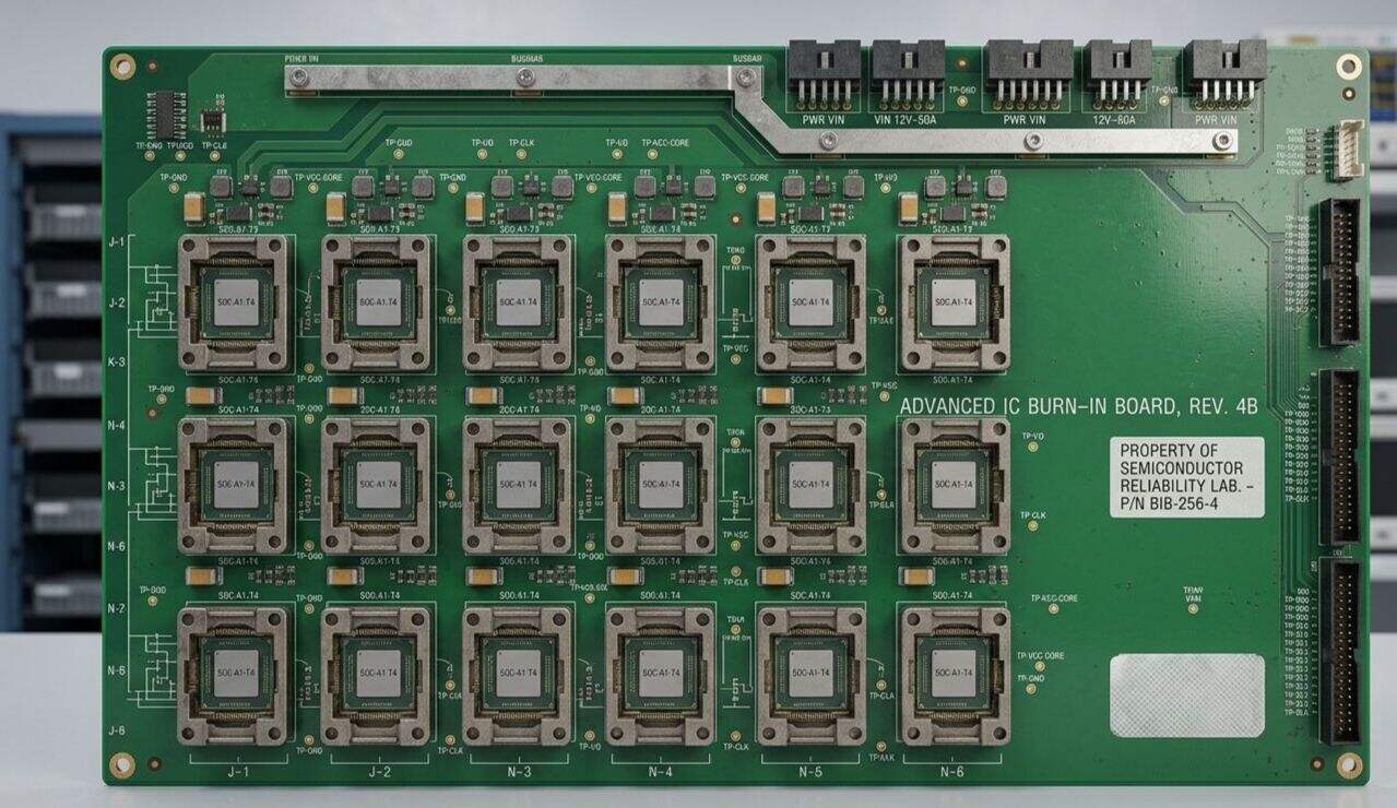
Quick Answers to Core Issues: What is a burn-in board (BIB)? Why is it prone to failure? A burn-in board (BIB) is a specialized interface hardware used for semiconductor burn-in testing. It subjects chips to prolonged stress conditions—including high temperature, high voltage, and dynamic signals—to screen out early-life failures. Key design challenges of BIBs include simultaneously ensuring uniform temperature distribution, signal integrity, power supply stability, and long-term mechanical reliability; any design flaw in these areas may distort test results or cause premature hardware failure.
Introduction
Burn-in testing is a critical method for semiconductor reliability validation, especially for applications demanding extremely high reliability—such as automotive electronics, industrial control, and aerospace systems. As the core hardware connecting the burn-in system to devices under test (DUTs), the burn-in board’s design quality directly impacts test result accuracy and system operational efficiency.
However, BIB design spans multiple disciplines—including materials science, thermodynamics, and electrical engineering—and designers frequently make mistakes at several key stages. This article analyzes these common errors one by one and provides practical avoidance methods.
Error One: Ignoring Material Fatigue Caused by Thermal Cycling
Problem Description
Burn-in testing typically runs continuously for several hours or even days at elevated temperatures, followed by cooling down to ambient temperature. Such repeated thermal cycling induces mechanical fatigue in BIB materials.
Many designers focus solely on a material’s temperature rating during selection, overlooking two equally critical parameters: coefficient of thermal expansion (CTE) matching and thermal fatigue resistance.
Common Consequences
- PCB interlayer delamination
- Solder joint cracking, leading to poor contact
- Aging and embrittlement of plastic components in sockets or connectors
- Reduced spring force in probes or pogo pins
Avoidance Methods
| Design Consideration | Recommended Practice |
|---|---|
| PCB Material Selection | Select high-Tg (glass transition temperature) materials, where Tg exceeds the maximum operating temperature of burn-in testing. Also consider the Z-axis CTE and select laminates with lower CTE values. |
| Copper Foil and Plating | Use highly ductile copper foil (e.g., rolled annealed copper) and apply wear-resistant, oxidation-resistant plating (e.g., hard gold). |
| Socket Selection | Select sockets validated for thermal cycling and review the supplier’s specified thermal cycle lifetime data. |
| Solder Joint Design | Apply underfill material to reinforce components subjected to mechanical or thermal stress. |
| Design Margin | In thermally sensitive areas, incorporate stress-relief structures instead of rigid fixation. |
Error Two: Inadequate Power Distribution Network (PDN) Impedance Design
Problem Description
During burn-in testing, multiple chips operate simultaneously, resulting in transient current demands significantly higher than those under standard room-temperature testing. Improper PDN impedance design on the BIB causes supply voltage fluctuations at the chip level, compromising test validity.
A common mistake is designing power trace widths and decoupling capacitor configurations based only on static current or average current, while neglecting the PDN impedance requirements imposed by transient current.
Common Consequences
- Chip supply voltage droop, causing unintended resets or functional anomalies
- Large voltage variations across different test sites, degrading test consistency
- Power noise coupling into signal paths, leading to misjudgment
Avoidance Methods
| Design Consideration | Recommended Practice |
|---|---|
| Current Estimation | Estimate peak current demand based on the chip’s datasheet maximum operating current and the specific dynamic test patterns used in burn-in testing. |
| Power Plane Design | Implement multi-layer power planes instead of single-width traces. Power planes should be as contiguous as possible, avoiding segmentation by signal traces. |
| Decoupling Capacitor Placement | Adopt a hierarchical placement strategy: large-capacitance capacitors near the power entry point, small-capacitance capacitors near chip power pins. |
| Kelvin Connection | For chips requiring precise voltage measurement, use four-wire Kelvin connections to eliminate measurement errors caused by contact resistance and trace resistance. |
| Simulation Validation | Perform PDN impedance simulation prior to fabrication to verify impedance compliance within the target frequency band. |
Error Three: Improper Signal Trace Length Matching Leading to Timing Skew
Problem Description
During burn-in testing, drive signals from the test system must travel through the BIB to reach the DUT, and output signals from the DUT must return via the BIB to the test system. Differences in propagation delay among signal channels can introduce timing skew—particularly critical for high-speed interfaces or parallel buses.
Common issues include designers failing to account for trace length differences across signal lines or ignoring delay contributions from vias and connectors.
Common Consequences
- Insufficient setup/hold time margin, causing data sampling errors
- Timing inconsistency across multiple test sites during parallel testing
- Eye diagram closure for high-frequency signals
Avoidance Methods
| Design Consideration | Recommended Practice |
|---|---|
| Length Matching | Strictly control length variation for signal groups with timing requirements (e.g., data bus, address bus). |
| Delay Calculation | Account for the PCB substrate’s dielectric constant when calculating actual signal propagation delay. |
| Via Impact | Vias introduce additional delay and impedance discontinuity; minimize via count on critical signal traces. |
| Connector Variation | Internal path lengths within connectors may vary across channels; evaluate this parameter during connector selection. |
| Simulation Validation | Perform timing simulation on critical signals to verify that setup/hold times meet chip specifications. |
Error Four: Socket Selection Without Considering Mechanical Lifetime
Problem Description
Burn-in boards undergo repeated insertion and removal of DUTs during testing; thus, socket mechanical lifetime directly determines BIB service life. Many designers prioritize electrical performance metrics (e.g., contact resistance, bandwidth) during socket selection, overlooking mechanical lifetime—a parameter equally critical.
During aging tests, chips may require multiple insertions and extractions under high-temperature conditions, placing higher demands on the socket’s material and structure.
Common Consequences
- Intermittent contact after prolonged use
- Changes in insertion/extraction force causing chip pin bending or socket damage
- Frequent socket replacement increasing maintenance costs and test downtime
Prevention Methods
| Design Considerations | Recommended Practices |
|---|---|
| Service Life Data | Review mechanical service life data (typically specified as insertion/extraction cycles) provided by suppliers during selection; choose models exceeding expected usage requirements |
| High-Temperature Performance | Verify performance of socket materials—especially plastic components—at aging test temperatures |
| Contact Force Design | Excessive contact force may damage chip pins; insufficient force may cause poor contact. Select proven design solutions |
| Replaceable Design | For sockets with limited mechanical service life, incorporate replaceability into the design to reduce repair complexity |
| Alternative Solutions | Maintain backup socket options for critical projects to accommodate supply chain or technical changes |
Error Five: Insufficient Maintainability Design Leading to High Repair Costs
Problem Description
BIBs inevitably experience failures during operation, including socket damage, connector contact issues, and component burnout. Without maintainability considerations in the design, repairs may become extremely difficult—even resulting in complete BIB scrapping.
Common issues include excessively dense component layout hindering disassembly, unexposed critical test points, and missing documentation.
Common Consequences
- Extended repair time causing test line downtime
- Damage to surrounding components during repair
- Inability to accurately locate faults leading to board-level scrap
- High repair costs, potentially exceeding new-unit manufacturing costs
Prevention Methods
| Design Considerations | Recommended Practices |
|---|---|
| Modular Design | Divide the BIB into functional modules (e.g., power supply, signal conditioning, interface modules) to facilitate fault isolation and replacement |
| Test Point Provision | Provide test points or vias at critical signal nodes to simplify fault diagnosis |
| Component Layout | Position fragile components (e.g., sockets, fuses) in easily accessible locations with sufficient surrounding workspace |
| Comprehensive Documentation | Provide complete repair manuals containing schematics, bill of materials, test point descriptions, and disassembly procedures |
| Maintainability Assessment | After BIB design completion, involve repair engineers to assess maintainability and identify potential issues early |
Comparison Table of Common Mistakes and Prevention Methods
| Common Mistake | Core Issue | Prevention Method |
|---|---|---|
| Ignoring thermal cycling effects on material fatigue | Inappropriate material selection and mismatched coefficients of thermal expansion (CTE) | Select high-Tg materials, ensure CTE matching, and incorporate stress-relief structures |
| Insufficient PDN impedance design | Underestimating transient current demands and improper decoupling strategy | Accurately estimate peak current, implement multi-layer power planes, and apply staged decoupling |
| Improper signal trace length matching | Neglecting transmission delay differences | Implement length-matching design, optimize via placement, and verify timing through simulation |
| Socket selection ignoring mechanical service life | Focusing solely on electrical performance while neglecting mechanical service life | Review service life data, confirm high-temperature performance, and design for replaceability |
| Lack of maintainability design | Dense layout, missing test points, incomplete documentation | Adopt modular design, provide test points, and supply comprehensive repair documentation |
Conclusion
Burn-in board design is a systems engineering task requiring balanced optimization across electrical performance, thermal management, mechanical reliability, and maintainability. Avoiding the five common mistakes outlined above significantly improves BIB test accuracy and service life while reducing long-term operational costs.
As a professional provider of ATE interface hardware, Semiroc has accumulated extensive experience in aging test board design. We offer end-to-end services—from concept design and simulation verification to manufacturing and delivery—helping customers mitigate design risks and accelerate time-to-market.
Contact our customer service team now to find answers to your questions.
CONTACT US