2026 Advanced Packaging Test Trends: How CPO, HBM4, and Glass Substrates Reshape ATE Interface Hardware
Key Insight: In 2026, the advanced packaging market is at a critical inflection point, with its value projected to reach approximately $47.88 billion. Driven by the massive computing demands of AI and High-Performance Computing (HPC), packaging is shifting from a simple “shell” for chips to a core methodology for system construction. This transformation introduces unprecedented customization challenges for ATE interface hardware.
Introduction
In 2026, advanced packaging is no longer a back-end process—it has become the defining factor in system performance. According to Mordor Intelligence, the advanced packaging market is expected to reach $47.88 billion. With AI compute demand continuing to surge, HBM4 entering mass production, and glass substrates alongside panel-level packaging moving toward industrialization, test interface hardware is facing a fundamental paradigm shift.
Traditional standardized ATE interfaces are no longer sufficient for 2026 test requirements. This article analyzes the five major strategic trends reshaping advanced packaging and explores their implications for test interface hardware, along with strategies to address them.
Five Strategic Trends in Advanced Packaging 2026 and Their Test Challenges
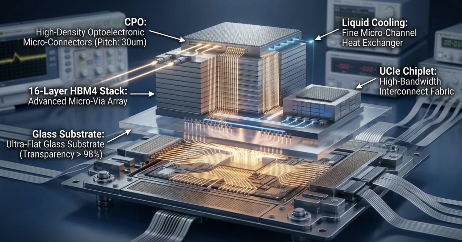
Trend 1: Co-Packaged Optics (CPO) Go Mainstream
Technology Background:
In 2026, CPO technology is accelerating toward commercialization, integrating optical engines directly at the package edge. This approach is expected to reduce network power consumption by up to 70%, making it a critical solution for hyperscale data centers grappling with AI networking power bottlenecks.
Test Challenges for ATE Interface Hardware:
- Optoelectronic Hybrid Testing: Requires simultaneous testing of high-speed electrical signals and optical interfaces—traditional purely electrical test interfaces are inadequate
- High-Frequency Signal Integrity: Optical engines at the package edge demand test interfaces with ultra-low insertion loss
- Multi-Physics Co-Simulation: Coupling of optical, electrical, and thermal domains requires probe cards and load boards with cross-domain simulation capabilities
Trend 2: HBM4 Mass Production Enables 16-Hi Stacking
Technology Background:
In 2026, HBM4 enters mass production with 16-layer vertical DRAM stacking (16-Hi) , delivering more than double the bandwidth of HBM3e to meet the ever-increasing bandwidth demands of AI model scaling.
Test Challenges for ATE Interface Hardware:
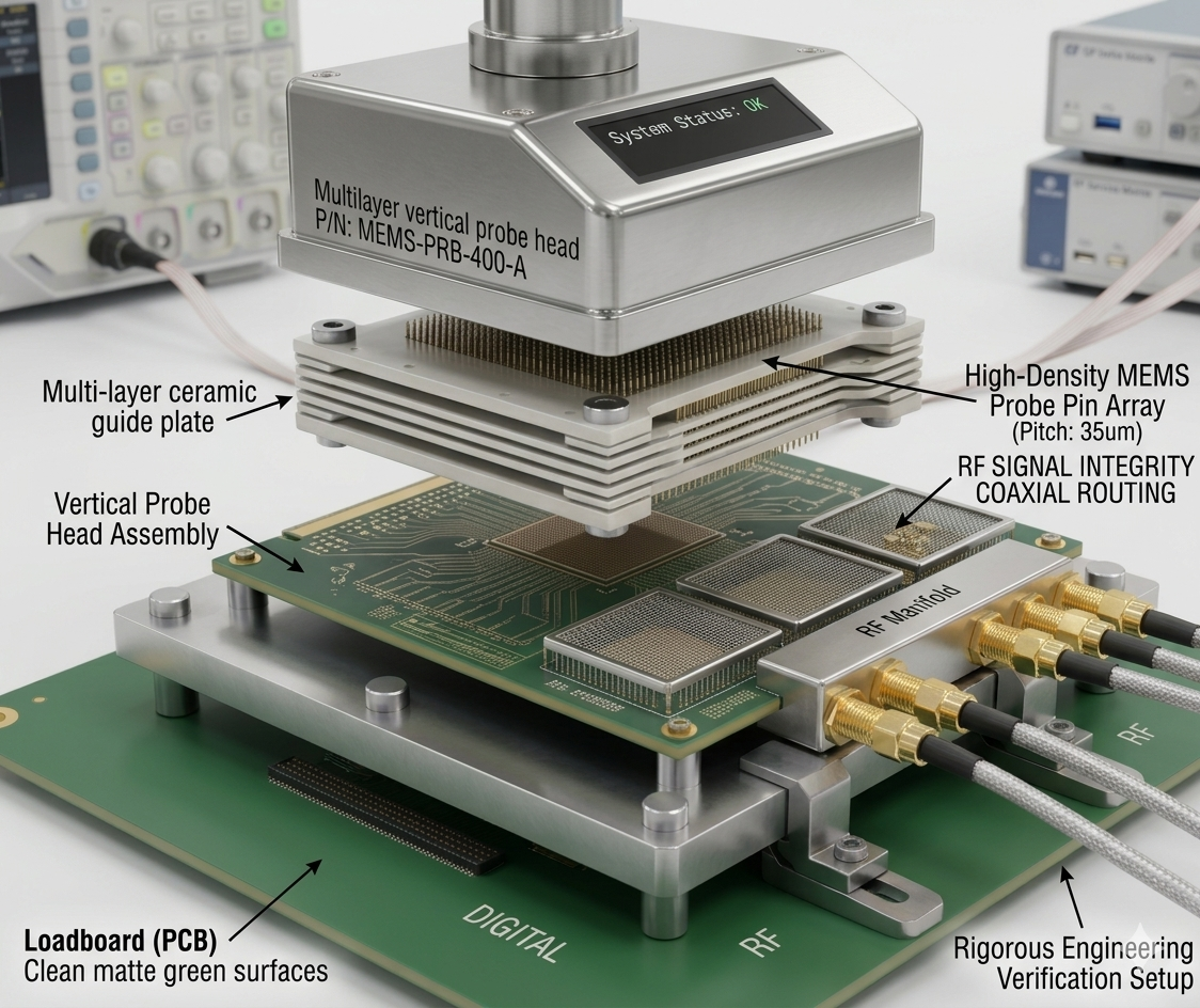
- Ultra-Fine Pitch Probes: With 16-Hi stacking, TSV pitch shrinks further, pushing MEMS probe accuracy and lifetime to their limits
- Ultra-High Parallel Testing: A single HBM stack requires testing thousands of TSVs, demanding probe cards with >1000 channels/mm² density
- Thermal Stress Management: 16-Hi stacking drives local heat flux density to extreme levels, requiring probe cards with thermal compensation designs to maintain contact stability under high temperatures
Trend 3: Transition to Glass Substrates and Panel-Level Packaging
Technology Background:
To overcome the size limitations of silicon interposers, the industry is accelerating its transition to glass-core substrates and panel-level packaging in 2026. Glass substrates offer superior flatness, tunable coefficient of thermal expansion (CTE), and larger form factors, making them a key enabler for next-generation advanced packaging.
Test Challenges for ATE Interface Hardware:
- CTE Matching Design: Glass substrates have CTE closer to silicon chips but significantly different from PCB materials. Load boards require gradient CTE transition structures
- Large-Format Warpage Control: Panel-level packaging can reach dimensions of 600mm × 600mm, demanding test interfaces with multi-point support and stiffener structures to maintain warpage
- New Test Contact Solutions: The surface characteristics of glass substrates differ from organic substrates, requiring new probe materials and contact force optimization
Trend 4: Breakthroughs in Thermal Management
Technology Background:
3D stacking drives power density to unprecedented levels, with local heat flux densities in AI chips reaching 200W/cm² in 2026. The industry is rapidly transitioning to liquid cooling, back-side power delivery, and advanced thermal interface materials.
Test Challenges for ATE Interface Hardware:
- Integrated Liquid Cooling Testing: Test interfaces must accommodate liquid cooling loop connections while maintaining sealing integrity during tri-temperature testing
- Back-Side Power Delivery Testing: Some advanced packages employ back-side power delivery networks (BSPDN), requiring test interfaces to contact both the front side (signals) and back side (power)—demanding dual-side probe capabilities
- Thermal Interface Material Compatibility: Test interfaces must adapt to new TIM materials without introducing thermal resistance drift during testing
Trend 5: Chiplet Architectures Penetrate Mobile Devices
Technology Background:
Chiplet architectures are beginning to penetrate the mobile market. According to TechInsights, smartphone processors (such as Apple’s A20) may adopt Chiplet designs in 2026, marking a shift away from traditional Package-on-PoP (PoP) architectures.
Test Challenges for ATE Interface Hardware:
- Multi-Die Interconnect Validation: Final test must validate interconnect quality between Chiplets (e.g., UCIe 2.0)
- Low-Power Test Adaptation: Mobile devices are sensitive to test power consumption, requiring optimization of test interface parasitic capacitance and inductance
- Mixed-Signal Test Complexity: Mobile chips integrate more RF and analog functions, demanding load boards with multi-domain signal isolation capabilities
Summary of 2026 Advanced Packaging Test Trends
| Strategic Trend | Key Technologies | Core Challenges for ATE Interface Hardware |
|---|---|---|
| Co-Packaged Optics | CPO, optoelectronic integration | Optoelectronic hybrid test, ultra-high-speed signal integrity |
| HBM4 Mass Production | 16-Hi stacking, TSV | Ultra-fine pitch probes, ultra-high parallel test |
| Glass Substrates | Glass core, panel-level packaging | CTE matching, large-format warpage control |
| Thermal Breakthroughs | Liquid cooling, back-side power delivery | Liquid cooling integration, dual-side contact test |
| Mobile Chiplet | Chiplet, UCIe | Multi-die interconnect validation, low-power test |
How Semiroc Addresses 2026 Advanced Packaging Test Challenges
As a specialized provider of ATE interface hardware, Semiroc has developed targeted solutions aligned with the key 2026 advanced packaging trends:
| Challenge | Solution | Key Technologies |
|---|---|---|
| CPO Optoelectronic Hybrid Test | Ultra-low loss high-frequency Load Boards | MLO and Rogers materials, insertion loss control, optoelectronic co-simulation |
| HBM4 16-Hi Stacking | High-density MEMS Probe Cards | Precise pitch, contact force control, tri-temperature support |
| Glass Substrate Test | CTE gradient adapter design | Multi-layer material transition structure, smaller warpage, large-panel support |
| Liquid Cooling Integration | Integrated thermal management interfaces | Liquid cooling loop compatibility, back-side power delivery probe cards, TIM validation |
| Mobile Chiplet Test | Multi-domain signal isolation Load Boards | High-speed digital/analog/RF partitioned design |
References
- Mordor Intelligence. (2026). High-End Semiconductor Packaging Market Forecasts 2031.
- TechInsights. (2026). 2026 Advanced Packaging Outlook Report.
- Yole Group. (2026). High-End Performance Packaging 2026.
- IDTechEx. (2026). Thermal Management for Advanced Semiconductor Packaging 2026-2036.
- Teradyne. (2025). UltraFLEX Platform Technical Overview.
Looking Ahead: Test Interfaces as a Core Competency in Advanced Packaging
In 2026, advanced packaging has evolved from “optional” to “essential.” Co-packaged optics, HBM4, glass substrates, liquid cooling integration, and mobile Chiplet architectures—these five trends all point to the same conclusion: test interfaces are no longer passive connectors but are deeply integrated with package design as a critical enabler.
For semiconductor manufacturers, selecting an interface supplier with proven 2026 advanced packaging test expertise will be a decisive factor in successful new product introduction.
Semiroc is ready to partner with you in addressing the challenges of advanced packaging test in 2026. Whether for CPO optoelectronic test, HBM4 16-Hi stacking, glass substrate adaptation, or kilowatt-class AI chip liquid cooling, we provide end-to-end support from simulation to manufacturing.
Contact our customer service team now to find answers to your questions.
CONTACT US