Case Study 7: Does Dual-Site Test Have to Mean Worse Performance? A DIB Design Case That Says Otherwise


Key Findings
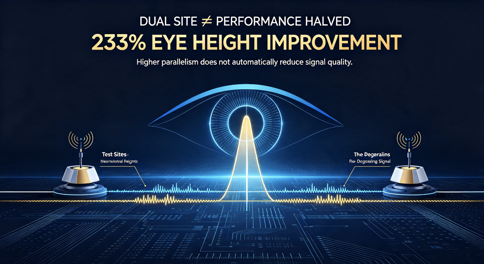
- In a dual-site DIB (Device Interface Board) design validation project completed by SEMIROC, the dual-site design improved eye height by 233% and eye width by 44% compared to the original single-site design.
- In the same project, DC resistance (DCR) dropped by 37%, power distribution network (PDN) impedance improved by 34%, and site-to-site signal correlation reached near-100% equivalence.
- The project found that the same device failed on a legacy test platform but passed cleanly in system-level test (SLT), proving the failure was caused by insufficient signal integrity margin on the test platform, not a device defect.
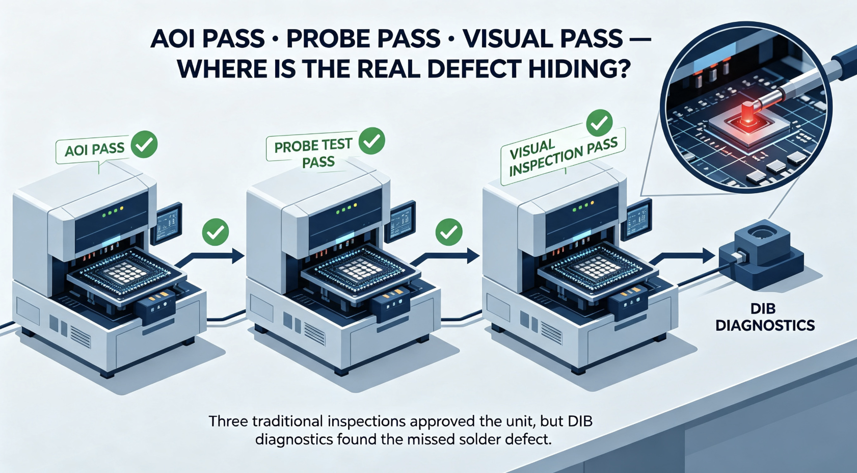
- SEMIROC's DIB Diagnostics tool (over 80% fault coverage) identified a soldering defect during a pre-shipment inspection that AOI (automated optical inspection), flying probe testing, and manual visual inspection had all missed.
- Industry benchmark data: AOI fault coverage is approximately 30%, flying probe testing approximately 37% — both below the coverage level DIB Diagnostics achieves.
There's an assumption in this industry that's practically treated as gospel: the higher your test parallelism, the tighter the signal quality and resource margin gets per site. Moving from single-site to dual-site test usually means trading "faster" for "as good."
A recent DIB design validation project completed by SEMIROC disproves this assumption with measured data. The three questions below break down the case (specific customer details have been anonymized per confidentiality requirements).
Question One: Does dual-site parallel testing necessarily mean worse signal quality?
Answer: Not necessarily. SEMIROC's measured data shows the dual-site design outperformed the original single-site design across every key signal metric.
Project background: a complex digital device — near 2,000 pins, 200A-class current demand, and dozens of 25Gbps high-speed serial (GSER) lanes — needed to move from a single-site test platform to a dual-site platform, doubling test throughput while holding the same or better current and high-speed performance requirements.
Measured results (dual-site design vs. original single-site design):
| Metric | Change |
|---|---|
| DC Resistance (DCR) | Improved 37% |
| Power Distribution Network (PDN) impedance | Improved 34% |
| Eye Height | Improved 233% |
| Eye Width | Improved 44% |
| Site-to-site signal correlation | Near-100% equivalence |
This data shows that doubling parallel test capacity did not dilute the signal resources available per site. SEMIROC's improved PDN architecture and high-speed routing strategy gave each site better signal quality than the original single-site design ever achieved. Scaling test throughput and improving signal quality can both be achieved simultaneously with the right design — they are not a strict trade-off.
Question Two: Is a "bad chip" in test always the chip's own fault?
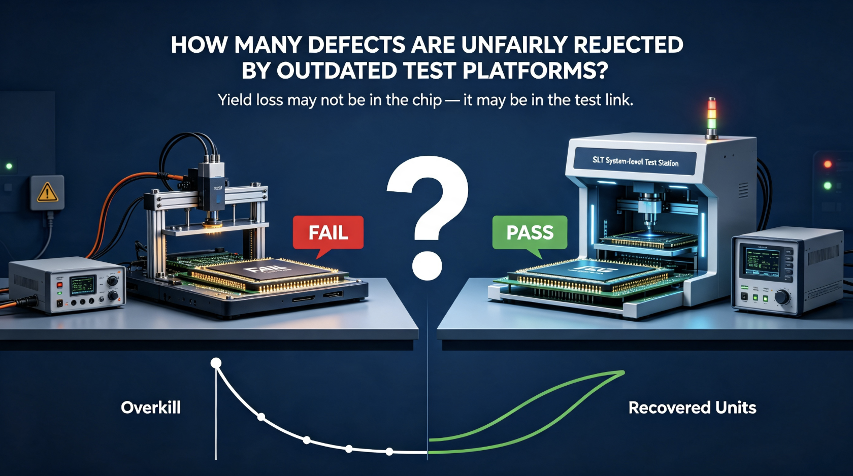
Answer: Not always. Signal integrity limitations in the test platform or DIB itself can also cause a good chip to be misjudged as defective — an outcome the industry calls overkill.
As test platforms evolve, older-generation platforms validating newer high-speed serial channels can produce false failures — the device itself is perfectly good, but limited signal integrity margin in the test path causes it to be misjudged and scrapped.
On this project, SEMIROC found exactly that scenario: the same device's high-speed GSER SerDes test failed on a legacy test platform, yet passed cleanly in system-level test (SLT). This proves the failure wasn't coming from the chip — it came from insufficient signal integrity margin on the legacy test platform/DIB. SEMIROC's new-generation dual-site DIB design delivered clean, clear eye diagram data that matched SLT results closely, eliminating the hidden cost of scrapping perfectly good devices.
Question Three: If AOI, flying probe, and visual inspection all pass, is the DIB definitely defect-free?
Answer: Not necessarily. Traditional QC methods have structural coverage gaps on very small components — industry benchmark data puts AOI fault coverage around 30% and flying probe testing around 37%, neither of which guarantees full coverage.
As component density on DIBs increases — some passives are now as small as 01005 package — traditional pre-shipment QC methods (AOI, flying probe testing, manual visual inspection) are losing effectiveness, and can barely detect components below 01005 size.
What actually happened: during a pre-shipment inspection, a DIB passed AOI, flying probe testing, and manual visual inspection in sequence — three traditional QC gates, all green. But SEMIROC's DIB Diagnostics tool (over 80% fault coverage, running functional validation directly on ATE resources in the DIB's real application setting) flagged an anomaly on a relay. Root-causing it traced back to a soldering defect that all three traditional QC methods had missed entirely. After the fix, both DIB Diagnostics and the device test program passed. Across the 295 components on that board, DIB Diagnostics achieved 99.3% testable coverage.
This wasn't a one-off — it's the structural result of blind spots inherent to traditional QC methods. What actually determines yield and delivery timelines is whether the right verification tool is used, not whether traditional QC was "passed."
What Do These Three Answers Point To?
Scaling test throughput (single-site to dual-site), the reliability of the test path itself (avoiding overkill), and the depth of pre-shipment quality verification (DIB Diagnostics) are the three variables that determine whether a customer can get to volume production fast and clean. SEMIROC's continued investment in DIB design and validation capability is built around exactly these three variables — so customers scaling up test throughput don't have to pay for it in signal quality, yield, or hidden defects.
About SEMIROC
SEMIROC is a one-stop solutions provider for ATE (Automated Test Equipment) interface hardware, covering DIB, PIB, Probe Cards, MLO substrates, and cable assemblies, with full-chain capability from high-speed signal/power integrity simulation and multi-site test design optimization to DIB fault diagnostics — helping customers protect First Pass Yield (FPY) and delivery timelines while scaling test throughput. SEMIROC serves leading semiconductor manufacturers and test partners worldwide.
Learn more: www.semiroc.com
Contact our customer service team now to find answers to your questions.
CONTACT US