
首页
关于我们
新闻中心
产品与服务
技术能力
ESG与可持续性管理
联系我们
English

技术能力

在ATE接口硬件的动态领域,我们的重点在于致力设计的持续发展,并与行业领先的上游合作伙伴进行战略合作。 这种协同的方法不仅确保了创新技术与我们产品的无缝集成,而且使我们处于不断发展的技术领域的前沿,推动我们提供不仅满足而且超越快速发展的行业需求的解决方案。

8月3日

2026年

高Site数MAP测试的层数效率与机械可靠性设计——SEMIROC技术能力解析

移动SoC量产测试正在把并测规模推向极致,大尺寸Panel、超高组件密度与紧凑的NPI周期同时挤压设计空间。SEMIROC解析如何用比同类方案减少约20%的PCB层数,同时保障信号/电源完整性与大尺寸Panel下的机械可靠性。
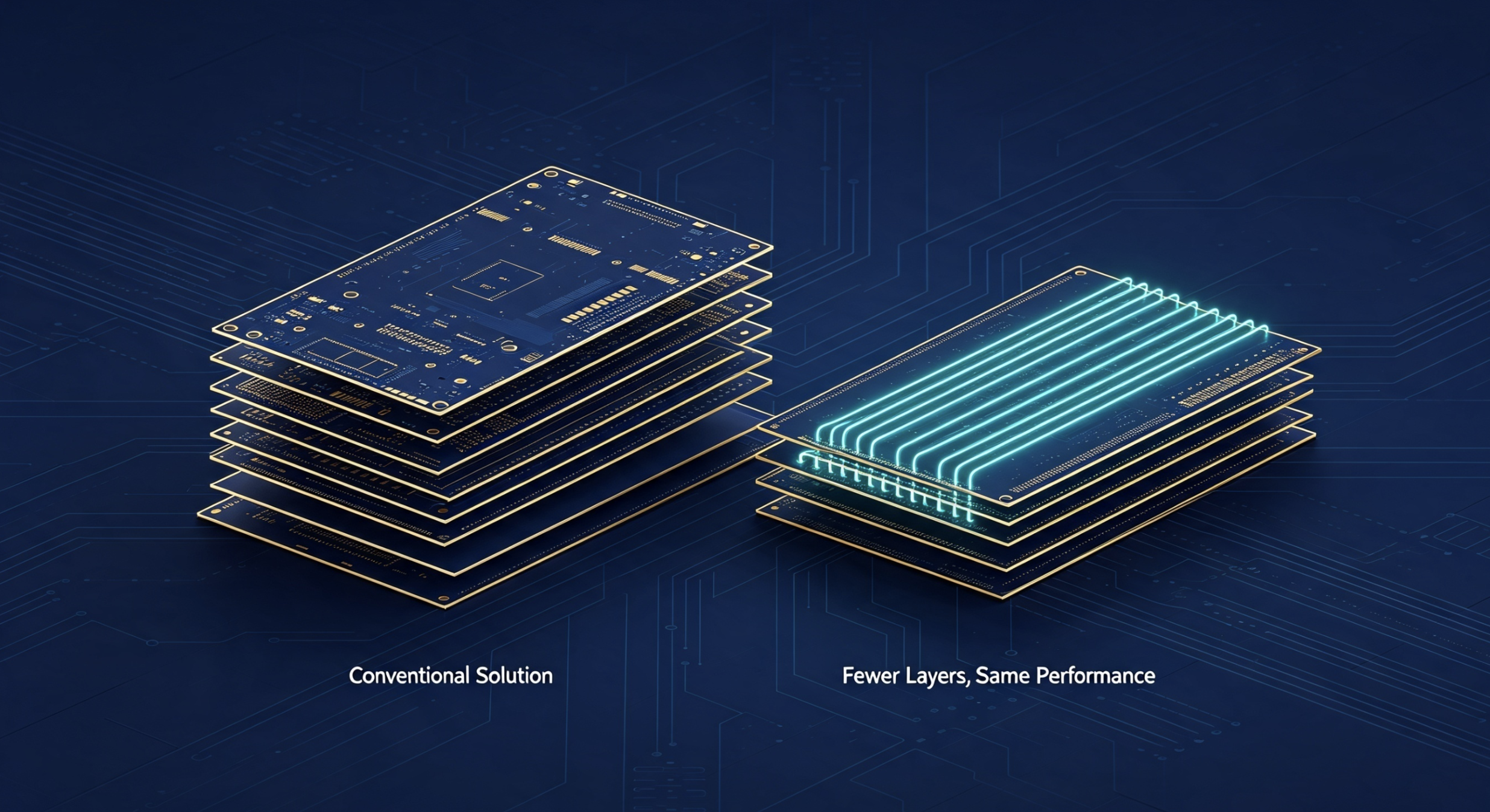
Side-by-side comparison of conventional vs. optimized circuit board stacks, highlighting fewer layers with same performance.
Close-up of a green-lit circuit board with microchips and intricate traces, evoking high-tech precision.
查看详情查看详情

7月22日

2026年

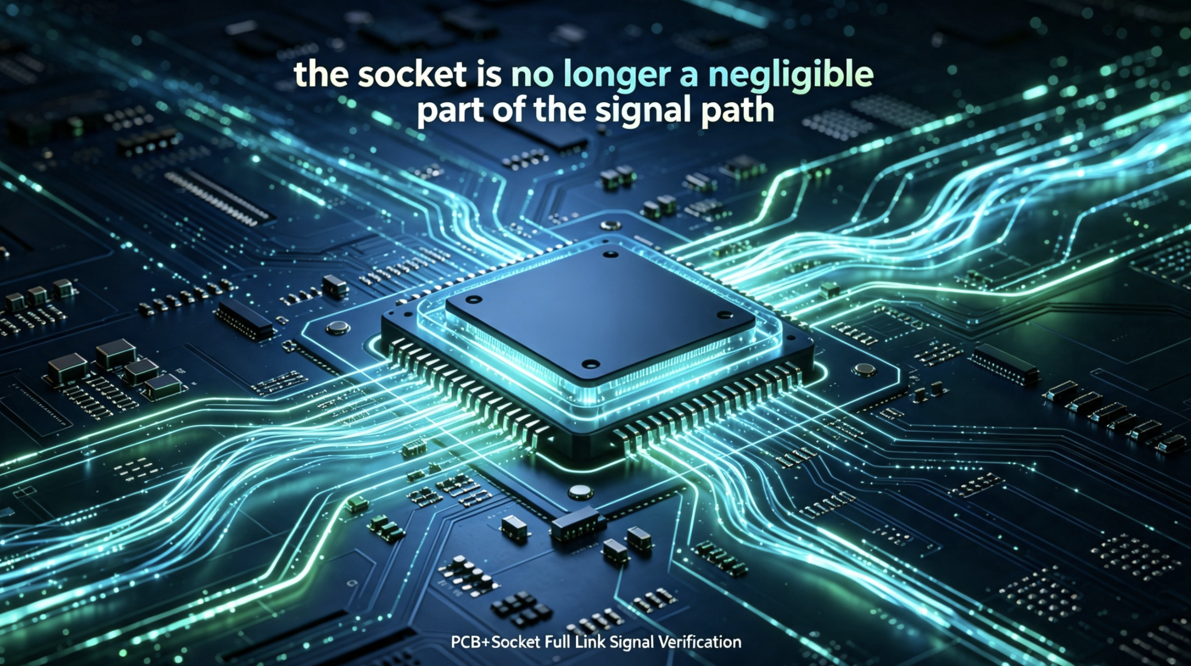
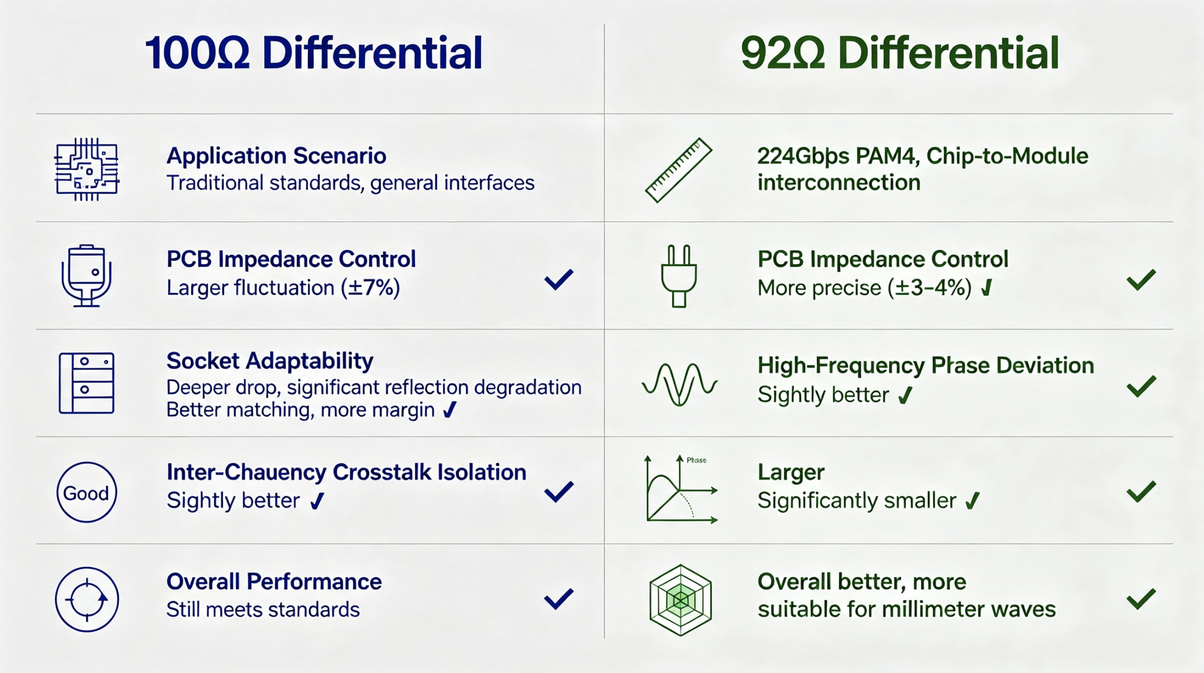
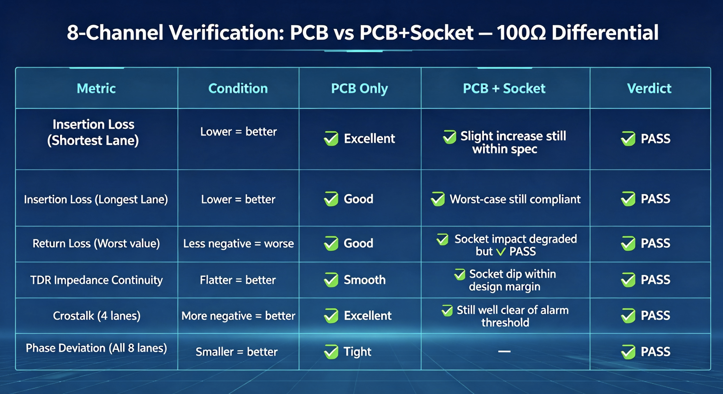
技术案例四:224Gbps毫米波测试的信号完整性设计 ——当信号速率迈入毫米波级别,"通孔"成了整个系统的短板

当测试信号速率迈入224Gbps毫米波级别,通孔阻抗不连续会直接劣化插入损耗与回波损耗,成为高频测试接口设计的第一道门槛。SEMIROC解析毫米波场景下的3D电磁建模、阻抗控制与探针协同设计能力。
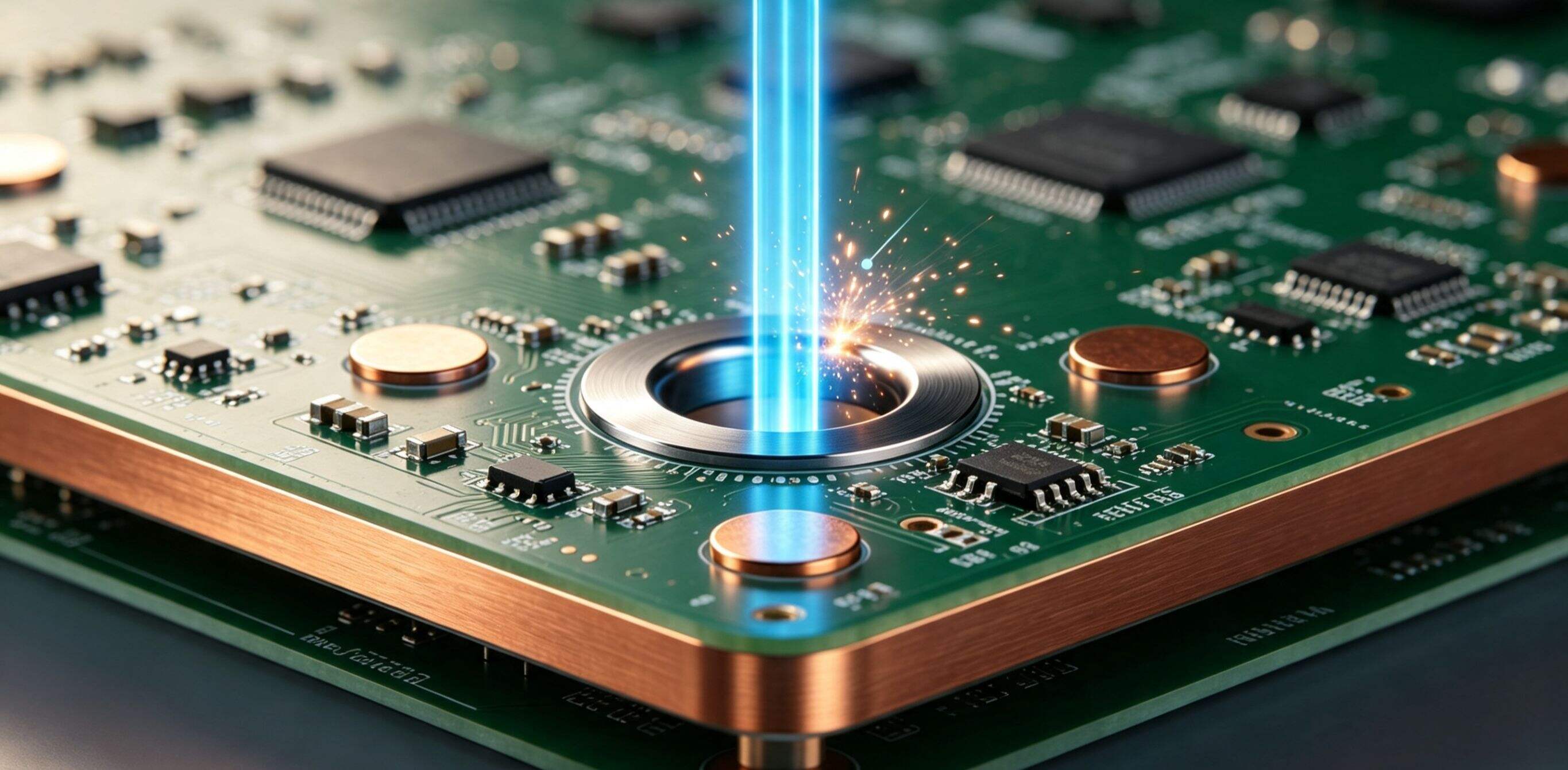
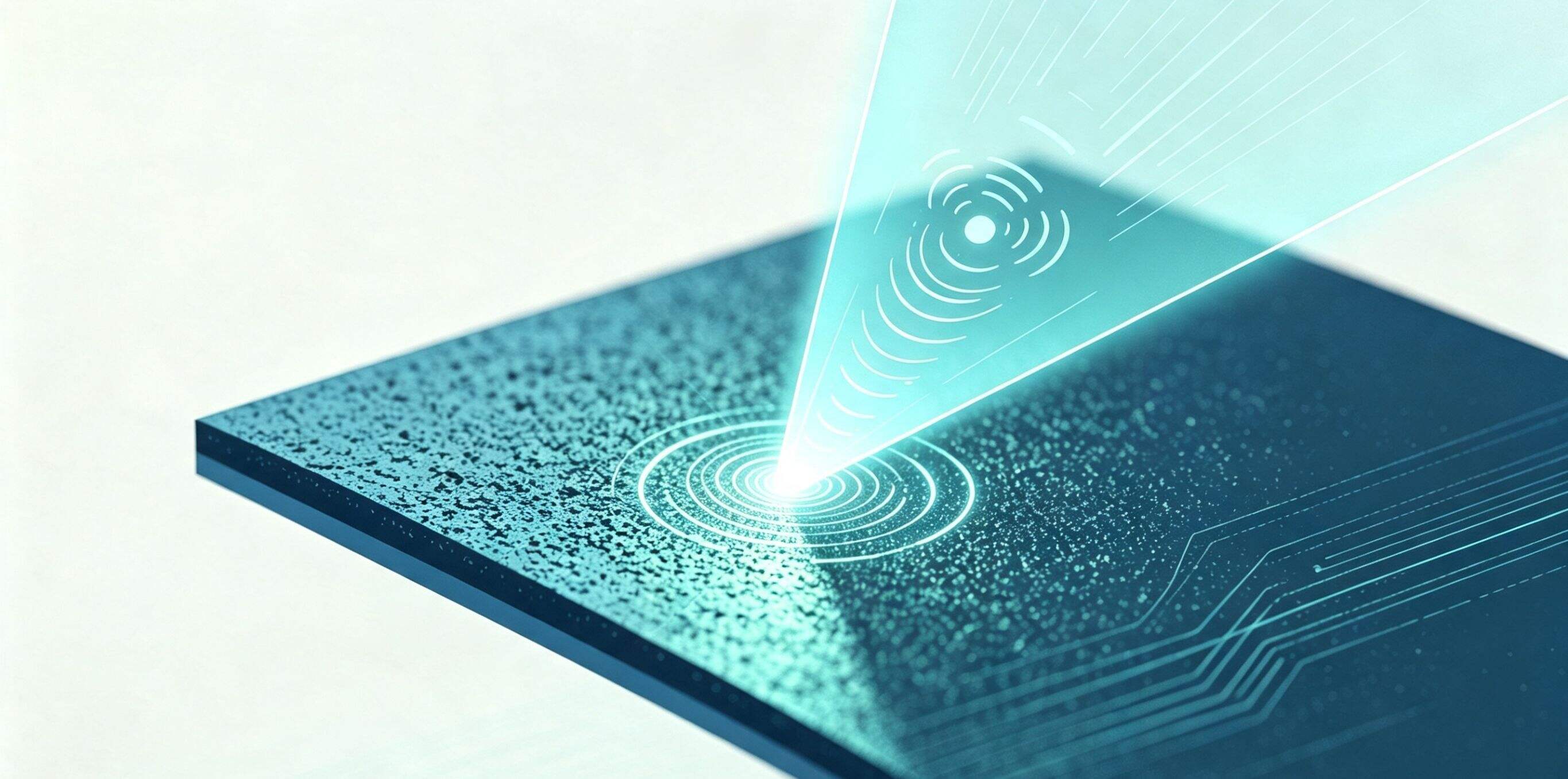
A green circuit board with a blue laser beam striking a central component, emitting sparksymbolizing advanced tech
A futuristic tech scene with a blue laser beam interacting with a circuit board, emitting concentric light waves.
查看详情查看详情

7月14日

2026年

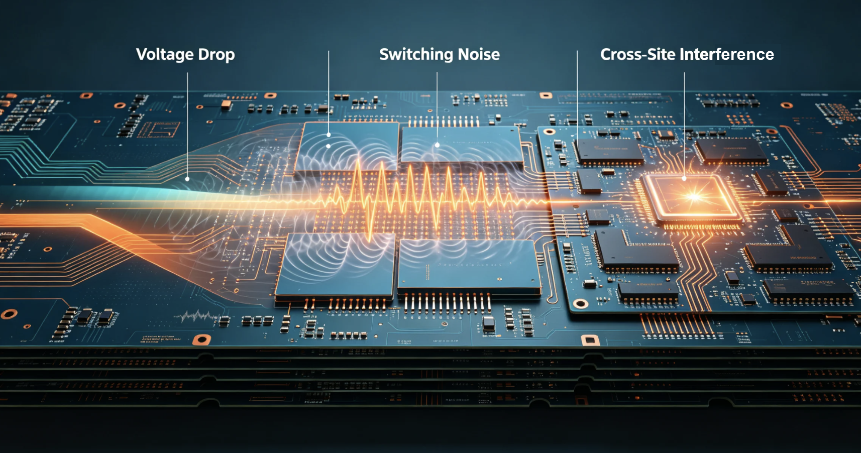
技术案例三:高密度多Site并测的电源完整性设计———当"并测数量"取代"单点电流",成为电源设计的第一变量

随着AI与高性能芯片测试普遍转向多Site并行以摊薄测试成本,电源完整性(PI)正在取代信号完整性成为设计瓶颈。SEMIROC解析领先的PI-driven设计方法论与平台能力,如何在高密度并测场景下保障接触稳定性与测试良率。

Glowing microchips on a circuit board with blue and green lighting, evoking advanced technology and digital innovation.
Technical illustration of a PCB showing voltage drop, switching noise, and cross-site interference with orange signal waves.
查看详情查看详情

7月6日

2026年

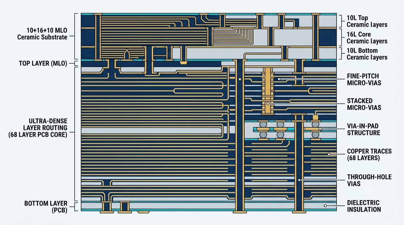
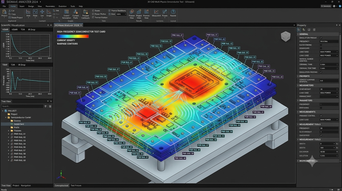
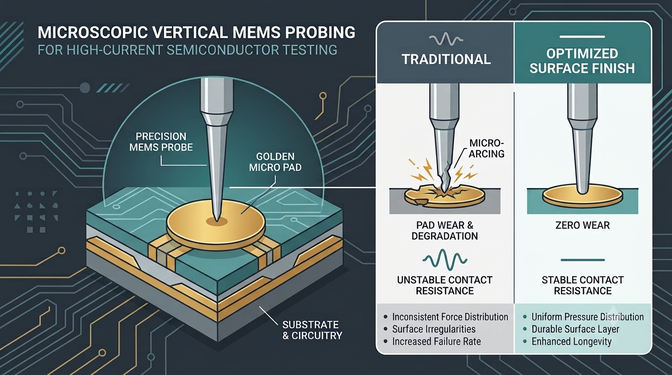
技术案例二:50GHz 高频与 5.4 万针极限密度——Semiroc 攻克 AI 混合信号芯片测试难题

Semiroc成功应对50GHz高频、5.4万针极限密度及高电流电源网络挑战,为AI/HPC芯片提供稳定可靠的晶圆级测试解决方案。
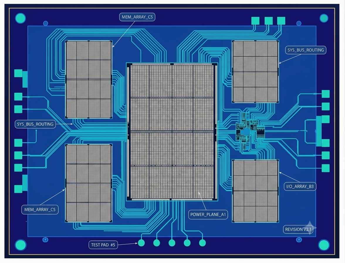
Blue printed circuit board layout with labeled components, routing traces, and memory arrays.
Technical diagram of a multilayer PCB with ultra-dense routing, copper traces, and stacked micro-vias.
3D thermal simulation of a circuit board in CAD software, showing heat distribution via color gradient.
Infographic comparing traditional vs optimized MEMS probing for testing, highlighting wear and contact stability.
查看详情查看详情

5月7日

2026年

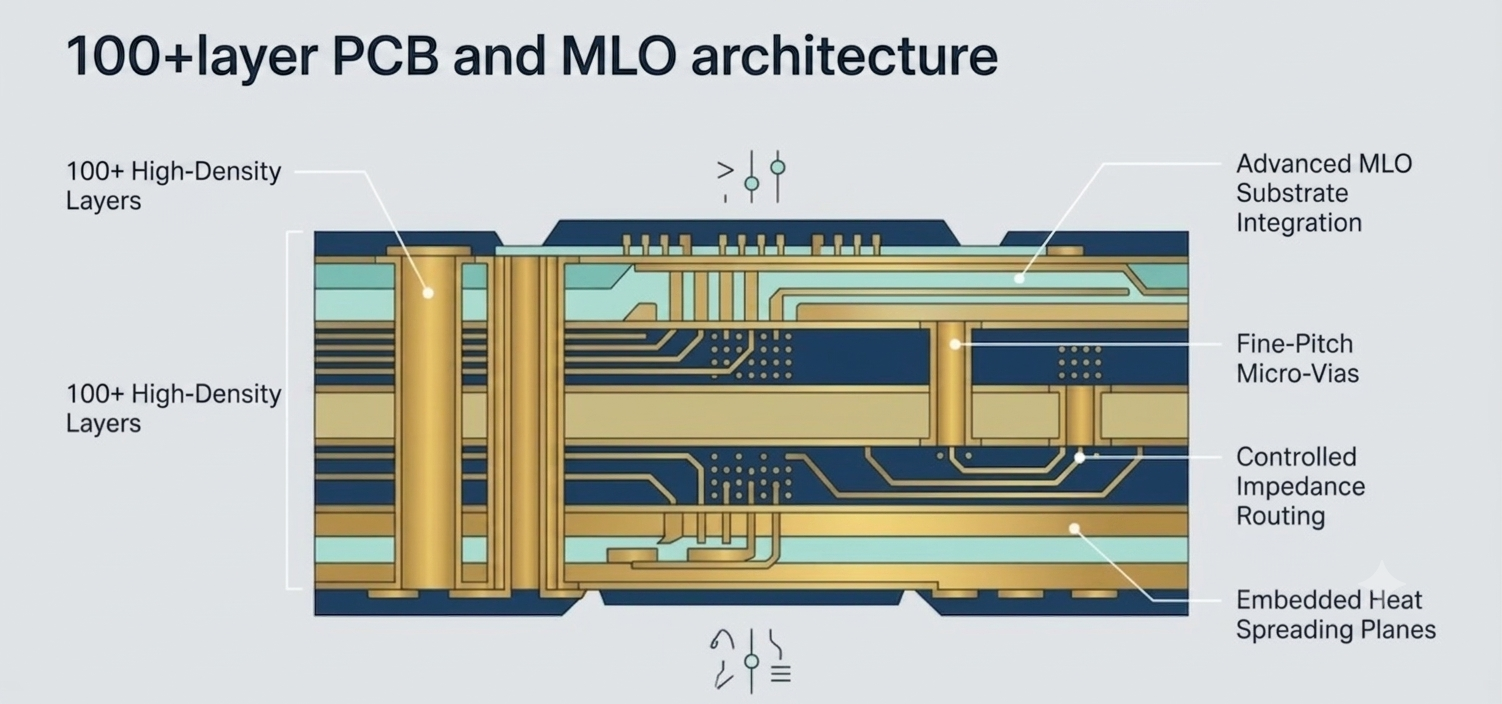
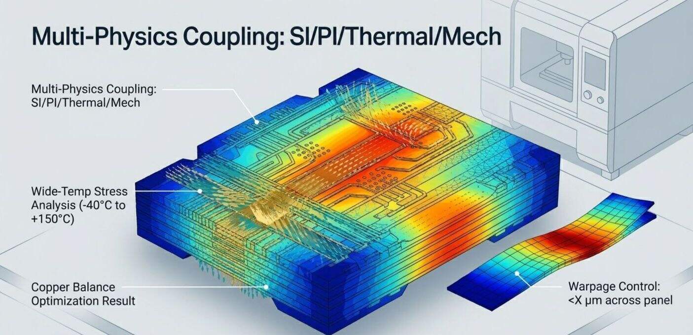
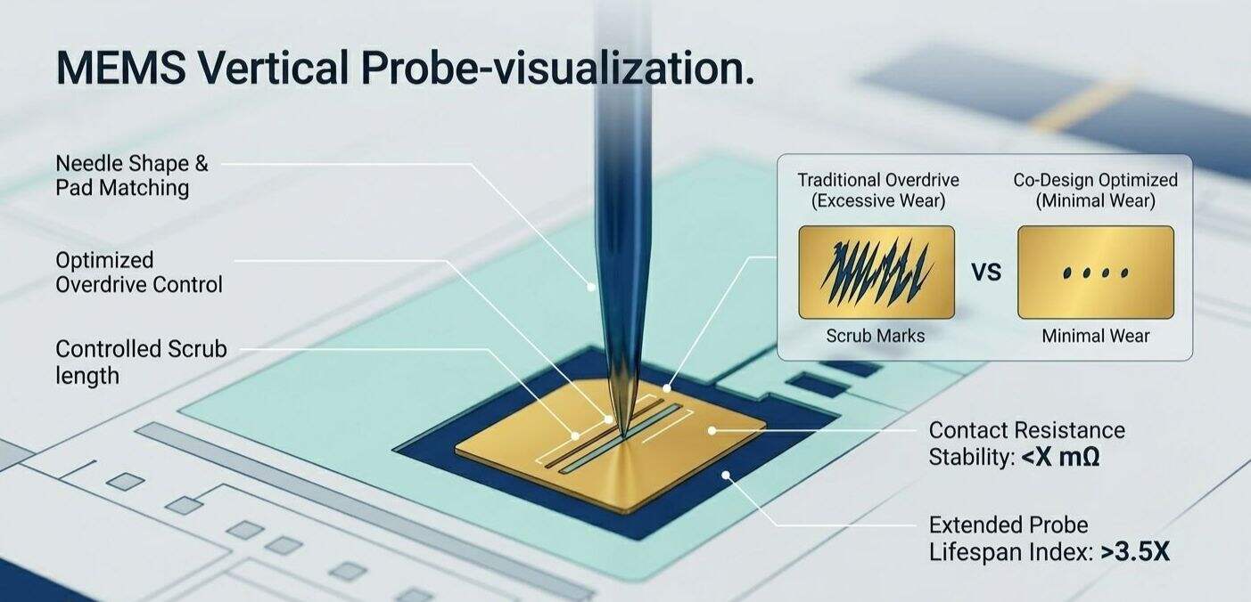
技术案例一:攻克 Chiplet 时代的并行测试极限 —— 120位超大规模垂直探测方案

针对下一代高性能计算(HPC)与AI芯片,Semiroc提供120+位超高并测垂直探针卡方案。通过100层高密度PCB与MLO协同设计,有效攻克宽温环境下Chiplet测试的良率挑战与机械翘曲难题。点击了解量产级SI/PI优化方案。
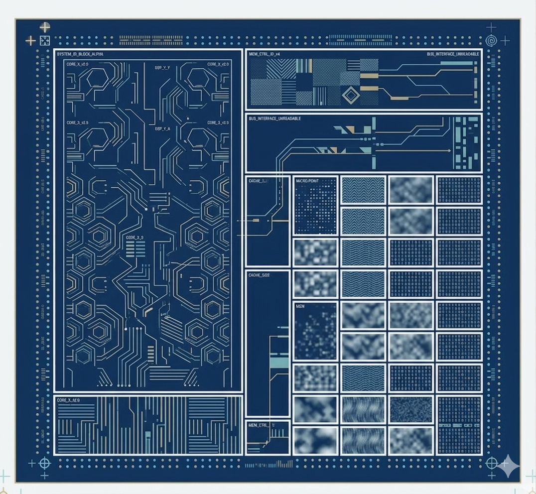
A futuristic blue circuit board schematic with hexagonal patterns, grids, and modular components.
Technical diagram of 100+ layer PCB and MLO architecture with labeled components.
3D multi-physics simulation of thermal, mechanical, and electrical coupling in chip packaging.
Technical diagram comparing traditional vs. co-design optimized MEMS vertical probes for semiconductor testing.
查看详情查看详情

4月7日

2026年

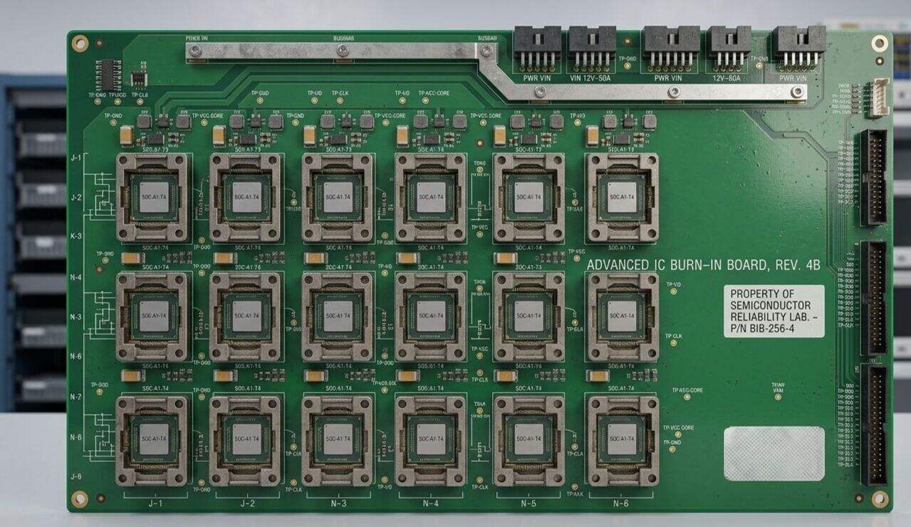
半导体老化测试板设计中的5个常见错误及避免方法

老化测试板设计中的五大常见错误:材料疲劳、PDN阻抗不足、信号线长匹配、插座选型、可维护性。提供实用的避免方法,提升BIB可靠性与寿命。
Green IC burn-in test board with 16 chip sockets, labeled for semiconductor reliability testing in a lab.
查看详情查看详情

3月26日

2026年

2026先进封装测试趋势:为什么ATE接口硬件需要定制化

2026年先进封装市场达478.8亿美元,CPO、HBM4 16层堆叠、玻璃基板驱动ATE测试接口定制化需求。解读光电混合测试、超细间距探针、液冷集成等新挑战。
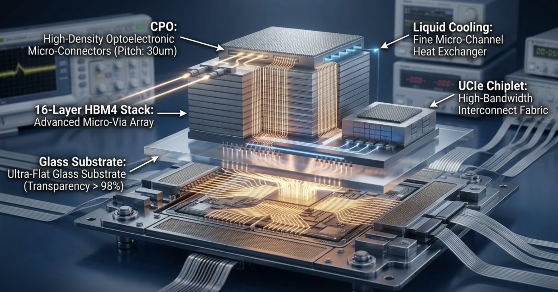
Advanced microchip architecture with labeled components, showcasing high-density connectors, liquid cooling, glass substrate.
High-precision MEMS probe station setup with labeled components for RF signal testing on PCB.
查看详情查看详情

3月23日

2026年

ATE负载板选型指南2026|从引脚数到可靠性

如何为Teradyne UltraFLEX、Advantest V93000选择ATE负载板?详解引脚数、信号完整性、电源完整性、热管理与供应商评估,助您提升首次通过率。
Close-up of a blue circuit board with an open CPU socket, showcasing intricate gold traces and electronic components.
Four graphs showing voltage vs. time with colored waveforms, illustrating signal patterns across different scales.
Infographic showing five key dimensions of supplier evaluation: technical manufacturing quality delivery value-added services
查看详情查看详情
查看更多

联系我们的客服团队解答您的问题!

联系我们
产品与服务
载板
探针卡
测试用线束
老化板
MLO测试板
加强筋
设计服务
一站式硬件解决方案
ATE PCB维修服务
关于我们
企业概况
企业文化
新闻中心
公司新闻
行业动态
联系我们
客户服务
提交询价
技术能力
技术更新
联系方式
地址: 上海市浦东新区秀浦路2555号A8栋505室
联系电话:8621-58185886
邮箱: sales@semiroc.com
网址: https://www.semiroc.com
Semiroc
|
Omron
沪ICP备2024051690号 |
隐私政策
|
使用条款
©上海莱翱电子科技有限公司 版权所有
Semiroc
|
Omron
沪ICP备2024051690号
隐私政策
|
使用条款
©上海莱翱电子科技有限公司 版权所有